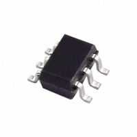
AD5641BKSZ-REEL7 Analog Devices Inc, AD5641BKSZ-REEL7 Datasheet

AD5641BKSZ-REEL7
Specifications of AD5641BKSZ-REEL7
Related parts for AD5641BKSZ-REEL7
AD5641BKSZ-REEL7 Summary of contents
Page 1
FEATURES 6-lead SC70 package Micropower operation: 100 μA maximum Power-down to typically 0.2 μ Single 14-bit DAC B version: ±4 LSB INL A version: ±16 LSB INL 2 5.5 V power supply ...
Page 2
AD5641 TABLE OF CONTENTS Features .............................................................................................. 1 Applications....................................................................................... 1 General Description ......................................................................... 1 Functional Block Diagram .............................................................. 1 Product Highlights ........................................................................... 1 Revision History ............................................................................... 2 Specifications..................................................................................... 3 Timing Characteristics ................................................................ 4 Absolute Maximum Ratings............................................................ 5 ESD Caution.................................................................................. 5 Pin ...
Page 3
SPECIFICATIONS kΩ to GND unless otherwise noted. Table 2. Parameter Min STATIC PERFORMANCE Resolution 14 1 Relative Accuracy 1 Differential Nonlinearity Zero-Code Error Offset Error Full-Scale Error ...
Page 4
AD5641 TIMING CHARACTERISTICS 5.5 V; all specifications T DD Table 3. 1 Parameter Limit 4 ...
Page 5
ABSOLUTE MAXIMUM RATINGS T = 25°C, unless otherwise noted. A Table 4. Parameter V to GND DD Digital Input Voltage to GND V to GND OUT Operating Temperature Range Industrial Storage Temperature Range Maximum Junction Temperature SC70 Package θ Thermal ...
Page 6
AD5641 PIN CONFIGURATION AND FUNCTION DESCRIPTIONS Table 5. Pin Function Descriptions Pin No. Mnemonic Description 1 SYNC Level-Triggered Control Input (Active Low). This is the frame synchronization signal for the input data. When SYNC goes low, it enables the input ...
Page 7
TYPICAL PERFORMANCE CHARACTERISTICS REF T = 25° –1 –2 –3 –4 256 2256 4256 6256 8256 10256 12256 14256 DAC CODE Figure 4. Typical INL 2.0 MAX INL ...
Page 8
AD5641 0.0025 0.0020 0.0015 ZERO-CODE ERROR @ V DD 0.0010 0.0005 ZERO-CODE ERROR @ V FULL-SCALE ERROR @ V 0 –0.0005 –0.0010 FULL-SCALE ERROR @ –0.0015 –0.0020 –0.0025 –40 – TEMPERATURE (°C) ...
Page 9
REF –1.2 –1.3 –1 REF –1.5 –1.6 –40 – TEMPERATURE (°C) ...
Page 10
AD5641 CH1 = SCLK CH1 = 5V/DIV CH2 = 1V/DIV TIME BASE = 2μs/DIV Figure 22. Full-Scale Settling Time CH1 = SCLK CH2 = V OUT CH1 = 5V/DIV CH2 = 1V/DIV TIME BASE = 2μs/DIV Figure 23. Midscale Settling ...
Page 11
CH1 V OUT CH2 CH1 5V, CH2 1V, TIME BASE = 2µs/DIV Figure 28. Exiting Power-Down Mode 140 FULL SCALE 120 100 1/4 SCALE 80 60 ZERO SCALE FREQUENCY (MHz) Figure 29. I ...
Page 12
AD5641 TERMINOLOGY Relative Accuracy For the DAC, relative accuracy or integral nonlinearity (INL measure of the maximum deviation, in LSBs, from a straight line passing through the endpoints of the DAC transfer function. See Figure 4 for a ...
Page 13
THEORY OF OPERATION DIGITAL-TO-ANALOG SECTION The AD5641 DAC is fabricated on a CMOS process. The architecture consists of a string DAC followed by an output buffer amplifier. Figure block diagram of the DAC architecture REF ...
Page 14
AD5641 DB15 (MSB) PD1 PD0 D13 SCLK SYNC SDIN DB15 INVALID WRITE SEQUENCE: SYNC HIGH BEFORE 16 FALLING EDGE TH POWER-ON RESET The AD5641 contains a power-on reset circuit that controls the output voltage during power-up. ...
Page 15
MICROPROCESSOR INTERFACING AD5641 to ADSP-2101 Interface Figure 37 shows a serial interface between the AD5641 and the ADSP-2101. The ADSP-2101 should be set up to operate in SPORT transmit alternate framing mode. The ADSP-2101 SPORT is programmed through the SPORT ...
Page 16
AD5641 APPLICATIONS CHOOSING A REFERENCE AS POWER SUPPLY FOR THE AD5641 The AD5641 comes in a tiny SC70 package with less than 100 μA supply current. Because of this, the choice of reference depends on the application requirement. For space-saving ...
Page 17
USING THE AD5641 WITH A GALVANICALLY ISOLATED INTERFACE In process control applications in industrial environments often necessary to use a galvanically isolated interface to protect and isolate the controlling circuitry from any hazardous common-mode voltages that might occur ...
Page 18
... AD5641 OUTLINE DIMENSIONS 0.10 MAX ORDERING GUIDE Temperature Model Range 1 AD5641AKSZ-REEL7 –40°C to +125°C 1 AD5641AKSZ-500RL7 –40°C to +125°C 1 AD5641BKSZ-REEL7 –40°C to +125°C 1 AD5641BKSZ-500RL7 –40°C to +125° RoHS Compliant Part. 2.20 2.00 1.80 1.35 2. 2.10 1.25 1. 1.80 PIN 1 ...
Page 19
NOTES Rev Page AD5641 ...
Page 20
AD5641 NOTES ©2005–2007 Analog Devices, Inc. All rights reserved. Trademarks and registered trademarks are the property of their respective owners. D04611-0-10/07(C) Rev Page ...


