AD625AD Analog Devices Inc, AD625AD Datasheet
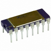
Instrumentation Amplifier IC

AD625AD

Manufacturer Part Number
AD625AD
Description
Instrumentation Amplifier IC
Manufacturer
Analog Devices Inc
Datasheet

Specifications of AD625AD

Gain Max, V/v
10000
Input Offset Voltage Max
200V
Supply Voltage Max
18V
Mounting Type
Through Hole
Supply Voltage Min
6V
Gain Min, V/v
1
Package / Case
16-CDIP
Rohs Status
RoHS non-compliant
Amplifier Type
Instrumentation
Number Of Circuits
1
Slew Rate
5 V/µs
Gain Bandwidth Product
25MHz
-3db Bandwidth
650kHz
Current - Input Bias
30nA
Voltage - Input Offset
50µV
Current - Supply
3.5mA
Voltage - Supply, Single/dual (±)
±6 V ~ 18 V
Operating Temperature
-40°C ~ 85°C
Output Type
-
Current - Output / Channel
-
Lead Free Status / RoHS Status

Available stocks

Company
Part Number
Manufacturer
Quantity
Price
Part Number:
AD625AD
Manufacturer:
ADI
Quantity:
439
Part Number:
AD625ADZ
Manufacturer:
AKM
Quantity:
1 400
Part Number:
AD625ADZ
Manufacturer:
Analog Devices Inc
Quantity:
135
Part Number:
AD625ADZ
Manufacturer:
ADI
Quantity:
439
a
PRODUCT DESCRIPTION
The AD625 is a precision instrumentation amplifier specifically
designed to fulfill two major areas of application: 1) Circuits re-
quiring nonstandard gains (i.e., gains not easily achievable with
devices such as the AD524 and AD624). 2) Circuits requiring a
low cost, precision software programmable gain amplifier.
For low noise, high CMRR, and low drift the AD625JN is the
most cost effective instrumentation amplifier solution available.
An additional three resistors allow the user to set any gain from
1 to 10,000. The error contribution of the AD625JN is less than
0.05% gain error and under 5 ppm/°C gain TC; performance
limitations are primarily determined by the external resistors.
Common-mode rejection is independent of the feedback resistor
matching.
A software programmable gain amplifier (SPGA) can be config-
ured with the addition of a CMOS multiplexer (or other switch
network), and a suitable resistor network. Because the ON
resistance of the switches is removed from the signal path, an
AD625 based SPGA will deliver 12-bit precision, and can be
programmed for any set of gains between 1 and 10,000, with
completely user selected gain steps.
For the highest precision the AD625C offers an input offset
voltage drift of less than 0.25 µV/°C, output offset drift below
15 µV/°C, and a maximum nonlinearity of 0.001% at G = 1. All
grades exhibit excellent ac performance; a 25 MHz gain band-
width product, 5 V/µs slew rate and 15 µs settling time.
The AD625 is available in three accuracy grades (A, B, C) for
industrial (–40°C to +85°C) temperature range, two grades (J,
K) for commercial (0°C to +70°C) temperature range, and one
(S) grade rated over the extended (–55°C to +125°C) tempera-
ture range.
√Hz
PRODUCT HIGHLIGHTS
1. The AD625 affords up to 16-bit precision for user selected
2. A 12-bit software programmable gain amplifier can be config-
3. The gain accuracy and gain temperature coefficient of the
4. The AD625 provides totally independent input and output
5. The proprietary design of the AD625 provides input voltage
6. External resistor matching is not required to maintain high
+INPUT
–INPUT
SENSE
SENSE
–GAIN
–GAIN
DRIVE
+GAIN
DRIVE
+GAIN
fixed gains from 1 to 10,000. Any gain in this range can be
programmed by 3 external resistors.
ured using the AD625, a CMOS multiplexer and a resistor
network. Unlike previous instrumentation amplifier designs,
the ON resistance of a CMOS switch does not affect the gain
accuracy.
amplifier circuit are primarily dependent on the user selected
external resistors.
offset nulling terminals for high precision applications. This
minimizes the effects of offset voltage in gain-ranging
applications.
noise of 4 nV/√Hz at 1 kHz.
common-mode rejection.
50
50
Instrumentation Amplifier
FUNCTIONAL BLOCK DIAGRAM
+
+
Programmable Gain
V
+
+
B
10k
10k
AD625
+
10k
10k
AD625
SENSE
OUTPUT
REFERENCE

Related parts for AD625AD

AD625AD Summary of contents

Page 1

PRODUCT DESCRIPTION The AD625 is a precision instrumentation amplifier specifically designed to fulfill two major areas of application: 1) Circuits re- quiring nonstandard gains (i.e., gains not easily achievable with devices such as the AD524 and AD624). 2) ...

Page 2

AD625–SPECIFICATIONS Model GAIN Gain Equation Gain Range 1 Gain Error Nonlinearity, Gain = 1-256 Gain>256 1 Gain vs. Temp. Gain<1000 GAIN SENSE INPUT Gain Sense Current vs. Temperature Gain Sense Offset Current vs. Temperature VOLTAGE OFFSET (May be Nulled) Input ...

Page 3

Model Min NOISE Voltage Noise, 1 kHz R.T.I. R.T.O. R.T.I., 0 100 G = 1000 Current Noise 0 SENSE INPUT ...

Page 4

... Differential Input Voltage . . . . . . . . . . . . . . . . . . . . . . . . . ± V Output Short Circuit Duration . . . . . . . . . . . . . . . . Indefinite Storage Temperature Range ( –65°C to +150°C Storage Temperature Range ( –65°C to +125°C Model Temperature Range AD625AD –40°C to +85°C AD625BD –40°C to +85°C AD625BD/+ –40°C to +85°C AD625CD – ...

Page 5

SUPPLY VOLTAGE – V –160 –140 G = 1000 G = 100 –120 –100 –80 –60 –40 – 100 ...

Page 6

AD625 –10 –20 –30 –40 –125 –75 – 125 TEMPERATURE – C 8.0 6.0 4.0 2 SUPPLY VOLTAGE – OUT AD625 10V –V ...

Page 7

– 1000 G = 100 – OUTPUT STEP – – 100 G = 1000 8 TO – –12 ...

Page 8

AD625 THEORY OF OPERATION The AD625 is a monolithic instrumentation amplifier based on a modification of the classic three-op-amp approach. Monolithic construction and laser-wafer-trimming allow the tight matching and tracking of circuit components. This insures the high level of performance ...

Page 9

Any resistors in series with the inputs of the AD625 will degrade the noise performance. For this reason the circuit in Figure 26b should be used if the gains are all greater than 5. For gains less than 5, either ...

Page 10

AD625 the I × R drops “inside the loop” and virtually eliminating this error source. Typically, IC instrumentation amplifiers are rated for a full ± 10 volt output swing into 2 kΩ. In some applications, however, the need exists to ...

Page 11

Offset voltage and offset voltage drift each have two compo- nents: input and output. Input offset is that component of offset that is generated at the input stage. Measured at the output it is directly proportional to gain, i.e., input ...

Page 12

AD625 GROUND RETURNS FOR BIAS CURRENTS Input bias currents are those currents necessary to bias the input transistors amplifier. There must be a direct return path for these currents, otherwise they will charge external capaci- tances, causing ...

Page 13

These capacitances may also be incorporated as part of the external input protection circuit (see section on Input Protec- tion general practice every effort should be made to match the extraneous capacitance at Pins 15 and 2, and ...

Page 14

AD625 1000 800 400 R 200 100 500 GAIN DETERMINING SPGA RESISTOR NETWORK VALUES The individual resistors in the gain network can be calculated sequentially ...

Page 15

Plastic DIP (N-16) 0.755 (19.18) 0.745 (18.93 0.26 (6.61) 0.24 (6. 0.306 (7.78) PIN 1 0.294 (7.47) 0.17 (4.32) MAX 0.175 (4.45) SEATING 0.12 (3.05) PLANE 0.02 (0.508) 0.015 (2.67) 0.065 (1.66) 0.015 (0.381) 0.095 ...

Related keywords