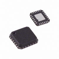
AD7147PACPZ-1RL Analog Devices Inc, AD7147PACPZ-1RL Datasheet - Page 35

AD7147PACPZ-1RL
Manufacturer Part Number
AD7147PACPZ-1RL
Description
CAPACITANCE TO DIGITAL CONVERTER
Manufacturer
Analog Devices Inc
Series
CapTouch™r
Type
Capacitive Sensor Controllerr
Datasheet
1.AD7147ACPZ-1500RL7.pdf
(72 pages)
Specifications of AD7147PACPZ-1RL
Resolution (bits)
16 b
Data Interface
I²C, Serial
Voltage Supply Source
Single Supply
Voltage - Supply
2.6 V ~ 3.6 V
Operating Temperature
-40°C ~ 85°C
Mounting Type
Surface Mount
Package / Case
24-LFCSP
Lead Free Status / RoHS Status
Lead free / RoHS Compliant
Sampling Rate (per Second)
-
Lead Free Status / Rohs Status
Compliant
SCLK
I
The AD7147-1 supports the industry standard 2-wire I
interface protocol. The two wires associated with the I
are the SCLK and SDA inputs. The SDA is an I/O pin that allows
both register write and register readback operations. The AD7147-1
is always a slave device on the I
It has a 7-bit device address, Address 0101 1XX. The lower two
bits are set by tying the ADD0 and ADD1 pins high or low. The
AD7147-1 responds when the master device sends its device
address over the bus. The AD7147-1 cannot initiate data trans-
fers on the bus.
Table 18. AD7147-1 I
ADD1
0
0
1
1
Data Transfer
Data is transferred over the I
The master initiates a data transfer by establishing a start con-
dition, defined as a high-to-low transition on the serial data
line, SDA, while the serial clock line, SCLK, remains high. This
indicates that an address/data stream follows.
SDO
2
SDI
C-COMPATIBLE INTERFACE
CS
NOTES
1. MULTIPLE REGISTERS CAN BE READ BACK CONTINUOUSLY.
2. THE 16-BIT CONTROL WORD MUST BE WRITTEN ON SDI: 5 BITS FOR ENABLE WORD, 1 BIT FOR R/W, AND 10 BITS FOR REGISTER ADDRESS.
3. THE ADDRESS AUTOMATICALLY INCREMENTS WITH EACH 16-BIT DATA-WORD BEING READ BACK ON THE SDO PIN.
4. CS IS HELD LOW UNTIL ALL REGISTER BITS HAVE BEEN READ BACK.
5. X DENOTES DON’T CARE.
6. XXX DENOTES HIGH IMPEDANCE THREE-STATE OUTPUT.
7. 16-BIT COMMAND WORD SETTINGS FOR SEQUENTIAL READBACK OPERATION:
XXX XXX XXX
CW
CW [15:11] = 11100 (ENABLE WORD)
CW [10] = 1 (R/W)
CW [9:0] = [AD9, AD8, AD7, AD6, AD5, AD4, AD3, AD2, AD1, AD0] (STARTING MSB-JUSTIFIED REGISTER ADDRESS)
15
1
ENABLE WORD
CW
14
2
CW
ADD0
0
1
0
1
13
3
XXX XXX XXX XXX XXX XXX XXX XXX XXX XXX
CW
12
2
C Device Address
4
CW
11
5
2
C serial interface in 8-bit bytes.
R/W
CW
2
10
C serial interface bus.
6
16-BIT COMMAND WORD
CW
9
I
0101 100
0101 101
0101 110
0101 111
2
7
C Address
CW
8
8
CW
7
9
REGISTER ADDRESS
CW
Figure 52. Sequential Register Readback SPI Timing
6
10
CW
5
11
2
C timing
2
C serial
CW
4
12
Rev. B | Page 35 of 72
CW
3
13
XXX XXX
CW
2
14
CW
1
15
All slave peripherals connected to the serial bus respond to the
start condition and shift in the next eight bits, consisting of a
7-bit address (MSB first) plus an R/ W bit that determines the
direction of the data transfer. The peripheral whose address
corresponds to the transmitted address responds by pulling the
data line low during the ninth clock pulse. This is known as the
acknowledge bit. All other devices on the bus then remain idle
while the selected device waits for data to be read from or written
to it. If the R/ W bit is 0, the master writes to the slave device. If
the R/ W bit is 1, the master reads from the slave device.
Data is sent over the serial bus in a sequence of nine clock
pulses—eight bits of data followed by an acknowledge bit from
the slave device. Transitions on the data line must occur during
the low period of the clock signal and remain stable during the
high period, because a low-to-high transition when the clock is
high can be interpreted as a stop signal. The number of data
bytes transmitted over the serial bus in a single read or write
operation is limited only by what the master and slave devices
can handle.
When all data bytes are read or written, a stop condition is
established. A stop condition is defined by a low-to-high
transition on SDA while SCLK remains high. If the AD7147
encounters a stop condition, it returns to its idle condition, and
the address pointer register resets to Address 0x00.
XXX
CW
0
16
D15
STARTING REGISTER ADDRESS
X
17
READBACK DATA FOR
D14
X
18
D1
X
31
D0
X
32
D15
X
33
NEXT REGISTER ADDRESS
READBACK DATA FOR
D14
X
34
D1
X
47
D0
X
48
AD7147
D15
X
49


