AD7265BSUZ-REEL7 Analog Devices Inc, AD7265BSUZ-REEL7 Datasheet - Page 14

AD7265BSUZ-REEL7
Manufacturer Part Number
AD7265BSUZ-REEL7
Description
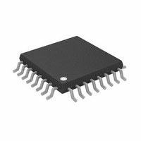
IC,Data Acquisition System,3-CHANNEL,12-BIT,TQFP,32PIN,PLASTIC
Manufacturer
Analog Devices Inc
Datasheet
1.AD7265BCPZ-REEL.pdf
(28 pages)
Specifications of AD7265BSUZ-REEL7
Design Resources
AD7265 in Differential and Single-Ended Configurations Using AD8022 (CN0048)
Number Of Bits
12
Sampling Rate (per Second)
1M
Data Interface
DSP, MICROWIRE™, QSPI™, Serial, SPI™
Number Of Converters
2
Power Dissipation (max)
21mW
Voltage Supply Source
Analog and Digital
Operating Temperature
-40°C ~ 125°C
Mounting Type
Surface Mount
Package / Case
32-TQFP, 32-VQFP
Lead Free Status / RoHS Status
Lead free / RoHS Compliant
For Use With
EVAL-AD7265CB - BOARD EVALUATION FOR AD7265
Lead Free Status / RoHS Status
Lead free / RoHS Compliant
Available stocks
Company
Part Number
Manufacturer
Quantity
Price
Company:
Part Number:
AD7265BSUZ-REEL7
Manufacturer:
Analog Devices Inc
Quantity:
10 000
Part Number:
AD7265BSUZ-REEL7
Manufacturer:
ADI/亚德诺
Quantity:
20 000
AD7265
When no amplifier is used to drive the analog input, the source
impedance should be limited to low values. The maximum source
impedance depends on the amount of THD that can be toler-
ated. The THD increases as the source impedance increases and
performance degrades.
the analog input signal frequency for different source impedances
in single-ended mode, while
analog input signal frequency for different source impedances
in differential mode.
Conversion Phase—Switches Open, Track Phase—Switches Closed
–50
–55
–60
–65
–70
–75
–80
–85
–90
–60
–65
–70
–75
–80
–85
–90
0
0
F
V
RANGE = 0V TO V
F
V
RANGE = 0V TO V
SAMPLE
DD
SAMPLE
DD
Various Source Impedances, Single-Ended Mode
= 3V
= 3V
Various Source Impedances, Differential Mode
Figure 19. THD vs. Analog Input Frequency for
Figure 20. THD vs. Analog Input Frequency for
Figure 18. Equivalent Analog Input Circuit,
V
V
100
100
R
= 1MSPS
IN+
IN–
= 1MSPS
SOURCE
R
C1
C1
SOURCE
R
SOURCE
REF
INPUT FREQUENCY (kHz)
INPUT FREQUENCY (kHz)
= 10Ω
200
REF
200
R
Figure 19 shows a graph of the THD vs.
SOURCE
= 0Ω
R
V
V
= 10Ω
SOURCE
DD
DD
D
D
D
D
Figure 20 shows the THD vs. the
= 47Ω
300
300
= 100Ω
400
400
R1 C2
R1 C2
R
R
R
SOURCE
SOURCE
SOURCE
R
R
SOURCE
SOURCE
500
500
= 300Ω
= 100Ω
= 300Ω
= 47Ω
= 0Ω
600
600
Rev. A | Page 14 of 28
Figure 21 shows a graph of the THD vs. the analog input
frequency for various supplies while sampling at 1 MSPS. In this
case, the source impedance is 47 Ω.
ANALOG INPUTS
The AD7265 has a total of 12 analog inputs. Each on-board
ADC has six analog inputs that can be configured as six single-
ended channels, three pseudo differential channels, or three
fully differential channels. These can be selected as described in
the
Single-Ended Mode
The AD7265 can have a total of 12 single-ended analog input
channels. In applications where the signal source has high
impedance, it is recommended to buffer the analog input before
applying it to the ADC. The analog input range can be pro-
grammed to be either 0 to V
If the analog input signal to be sampled is bipolar, the internal
reference of the ADC can be used to externally bias up this
signal to make it correctly formatted for the ADC. Figure 22
shows a typical connection diagram when operating the ADC
in single-ended mode.
+1.25V
–1.25V
Figure 21. THD vs. Analog Input Frequency for Various Supply Voltages
Analog Input Selection section.
0V
–50
–55
–60
–65
–70
–75
–80
–85
–90
0
F
V
RANGE = 0 TO V
SAMPLE
Figure 22. Single-Ended Mode Connection Diagram
DD
= 3V/5V
100
= 1MSPS
V
SINGLE-ENDED MODE
DD
V
IN
= 5V
1
REF
ADDITIONAL PINS OMITTED FOR CLARITY.
INPUT FREQUENCY (kHz)
200
3R
R
R
REF
or 0 to 2 × V .
300
R
+2.5V
V
DIFFERENTIAL MODE
DD
0V
V
SINGLE-ENDED MODE
V
DIFFERENTIAL MODE
400
DD
DD
= 3V
= 3V
= 5V
V
V
REF
A1
B6
500
D
CAP
AD7265
A/D
CAP
0.47µF
600
1
B


