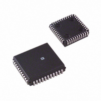
AD7716BPZ Analog Devices Inc, AD7716BPZ Datasheet - Page 10

AD7716BPZ
Manufacturer Part Number
AD7716BPZ
Description
4-CHNL S-D ADC
Manufacturer
Analog Devices Inc
Datasheet
1.AD7716BP-REEL.pdf
(16 pages)
Specifications of AD7716BPZ
Number Of Bits
22
Sampling Rate (per Second)
2.23k
Data Interface
Serial
Number Of Converters
4
Power Dissipation (max)
50mW
Voltage Supply Source
Analog and Digital, Dual ±
Operating Temperature
-40°C ~ 85°C
Mounting Type
Surface Mount
Package / Case
44-PLCC
Lead Free Status / RoHS Status
Lead free / RoHS Compliant
For Use With
EVAL-AD7716EBZ - BOARD EVAL FOR AD7716
Lead Free Status / RoHS Status
Lead free / RoHS Compliant
Available stocks
Company
Part Number
Manufacturer
Quantity
Price
Company:
Part Number:
AD7716BPZ
Manufacturer:
ST
Quantity:
2 100
Company:
Part Number:
AD7716BPZ
Manufacturer:
Analog Devices Inc
Quantity:
10 000
AD7716
relationship between input bandwidth and settling is given in
Table I. Because of this settling time, most sigma delta ADCs
are unsuitable for high speed multiplexing, where channels are
switched and converted sequentially at high rates, as switching
between channels can cause a step change in the input.
ever, the AD7716 is a sigma-delta solution to multichannel ap-
plications, since it can process four channels simultaneously. In
addition, it is easy to cascade several devices in order to increase
the number of channels being processed.
Figure 6 shows the filter frequency response for a cutoff fre-
quency of 73 Hz. This is a (sinx/x)
that provides greater than 100 dB rejection at the notch fre-
quencies. The relationship between the programmed cutoff
frequency and the first notch is constant (f
f
The settling time to a full-scale step input is four times the out-
put data period. Programming a different cutoff frequency via
FC0–FC2 does not alter the profile of the filter response, it sim-
ply changes the frequency of the notches.
In Figure 6, the first notch is at 278 Hz. This is also the output
data rate. Settling time to a full-scale step input is 10.8 ms.
The digital filter can be defined by the following equations.
where N = Ratio of Modulator Sampling Frequency to Output
and
CUTOFF
Figure 6. Frequency Response of AD7716 Filter
f
). The first notch frequency is also the output data rate.
S
= Output Rate.
–100
–120
–140
–160
–180
–200
–220
–240
–20
–40
–60
–80
Rate
0
0
73
H (z)
H ( f )
278
FREQUENCY – Hz
556
N
1
sin f / f
1– Z
f / f
1– Z
834
3
response (also called sinc
S
S
)
– N
–1
)
1112
NOTCH
3
3
1390
= 3.81
1668
How-
3
)
–10–
Post Filtering
In the AD7716, the on-chip modulator provides the digital filter
with samples at a rate of 570 kHz. The filter decimates these
samples to provide data at an output rate which corresponds to
the programmed first notch frequency of the filter.
If the user wants to reduce the output noise from the device for
bandwidths less than 36.5 Hz, then it is possible to employ extra
filtering after the AD7716. This extra digital filtering is called
post filtering. If a straight averaging filter is used, for example, a
reduction in bandwidth by a factor of 2 results in 2 reduction
in the rms noise. This additional filtering will also result in a
longer settling time.
Antialias Considerations
The digital filter does not provide any rejection at integer mul-
tiples of the modulator sampling frequency (n
where n = 1, 2, 3, . . .). This means that there are frequency
bands, f
to FC2) where noise passes unattenuated to the output. How-
ever, due to the AD7716’s high oversampling ratio, these bands
occupy only a small fraction of the spectrum and most broad-
band noise is filtered.
In spectral analysis applications, it is important to note that at-
tenuation at half the output update rate is 16 dB. Extra front-
end filtering or post filtering may be required to keep aliases in
this frequency band at an acceptable level.
USING THE AD7716
SYSTEM DESIGN CONSIDERATIONS
The AD7716 operates differently from successive approxima-
tion ADCs or other integrating ADCs. Since it samples the sig-
nal continuously, like a tracking ADC, there is no need for a
start convert command. The output register is updated at a rate
dependent on the programmed cutoff frequency, and the output
can be read at any time.
Input Signal Conditioning
The input range for the AD7716 is V
nal conditioning. This may take the form of gain to increase a
smaller signal range, or passive attenuation to reduce a larger in-
put voltage range.
10%. Other input ranges can be accommodated by input sig-
3dB
wide (f
3dB
is the cutoff frequency selected by FC0
REF
, where V
570 kHz,
REF
= 2.5 V
REV. A


