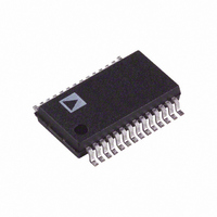
AD7899ARSZ-2 Analog Devices Inc, AD7899ARSZ-2 Datasheet - Page 9

AD7899ARSZ-2
Manufacturer Part Number
AD7899ARSZ-2
Description
14-BIT BIPOLAR INPUT SINGLE SUPPLY ADC
Manufacturer
Analog Devices Inc
Datasheet
1.AD7899ARSZ-1.pdf
(16 pages)
Specifications of AD7899ARSZ-2
Number Of Bits
14
Sampling Rate (per Second)
400k
Data Interface
Parallel
Number Of Converters
1
Power Dissipation (max)
125mW
Voltage Supply Source
Single Supply
Operating Temperature
-40°C ~ 85°C
Mounting Type
Surface Mount
Package / Case
28-SSOP (0.200", 5.30mm Width)
Number Of Elements
1
Resolution
14Bit
Architecture
SAR
Sample Rate
400KSPS
Input Polarity
Unipolar
Input Type
Voltage
Rated Input Volt
2.5/5V
Differential Input
No
Power Supply Requirement
Single
Single Supply Voltage (typ)
5V
Single Supply Voltage (min)
4.75V
Single Supply Voltage (max)
5.25V
Dual Supply Voltage (typ)
Not RequiredV
Dual Supply Voltage (min)
Not RequiredV
Dual Supply Voltage (max)
Not RequiredV
Power Dissipation
125mW
Differential Linearity Error
±1LSB
Integral Nonlinearity Error
±2LSB
Operating Temp Range
-40C to 85C
Operating Temperature Classification
Industrial
Mounting
Surface Mount
Pin Count
28
Package Type
SSOP
Input Signal Type
Single-Ended
Lead Free Status / RoHS Status
Lead free / RoHS Compliant
For Use With
EVAL-AD7899CBZ - BOARD EVAL FOR AD7899
Lead Free Status / Rohs Status
Compliant
Available stocks
Company
Part Number
Manufacturer
Quantity
Price
Part Number:
AD7899ARSZ-2
Manufacturer:
ADI/亚德诺
Quantity:
20 000
For the AD7899-1, R1 = 4 kΩ, R2 = 16 kΩ, R3 = 16 kΩ and
R4 = 8 kΩ. The resistor input stage is followed by the high
input impedance stage of the track/hold amplifier.
The designed code transitions take place midway between suc-
cessive integer LSB values (i.e., 1/2 LSB, 3/2 LSBs, 5/2 LSBs
etc.) LSB size is given by the formula, 1 LSB = FSR/16384. For
the ±5 V range, 1 LSB = 10 V/16384 = 610.4 µV. For the ±10 V
range, 1 LSB = 20 V/16384 = 1.22 mV. Output coding is
two’s complement binary with 1 LSB = FSR/16384. The ideal
input/output transfer function for the AD7899-1 is shown in
Table I.
Analog Input
+FSR/2 – 3/2 LSB
+FSR/2 – 5/2 LSB
+FSR/2 – 7/2 LSB
GND + 3/2 LSB
GND + 1/2 LSB
GND – 1/2 LSB
GND – 3/2 LSB
–FSR/2 + 5/2 LSB
–FSR/2 + 3/2 LSB
–FSR/2 + 1/2 LSB
NOTES
1
2
FSR is full-scale range and is 20 V for the ±10 V range and 10 V for the ±5 V
1 LSB = FSR/16384 = 1.22 mV (±10 V – AD7899-1) and 610.4 µV (±5 V –
range, with V
AD7899-1) with V
Table I. Ideal Input/Output Code Table for the AD7899-1
V
V
V
REF
INB
INA
REF
6k
1
= 2.5 V.
REF
= 2.5 V.
2
R2
R3
REFERENCE
R1
R4
2.5V
GND
Digital Output
Code Transition
011 . . . 110 to 011 . . . 111
011 . . . 101 to 011 . . . 110
011 . . . 100 to 011 . . . 101
000 . . . 001 to 000 . . . 010
000 . . . 000 to 000 . . . 001
111 . . . 111 to 000 . . . 000
111 . . . 110 to 111 . . . 111
100 . . . 010 to 100 . . . 011
100 . . . 001 to 100 . . . 010
100 . . . 000 to 100 . . . 001
TRACK/HOLD
TO ADC
REFERENCE
CIRCUITRY
AD7899-1
TO INTERNAL
COMPARATOR
AD7899-2
Figure 3 shows the analog input section of the AD7899-2. Each
input can be configured for 0 V to 5 V operation or 0 V to 2.5 V
operation. For 0 V to 5 V operation, the V
GND and the input voltage is applied to the V
0 V to 2.5 V operation, the V
and the input voltage is applied to both. The V
inputs are symmetrical and fully interchangeable.
For the AD7899-2, R1 = 4 kΩ and R2 = 4 kΩ. Once again, the
designed code transitions occur on successive integer LSB values.
Output coding is straight (natural) binary with 1 LSB = FSR/
16384 = 2.5 V/16384 = 0.153 mV, and 5 V/16384 = 0.305 mV,
for the 0 to 2.5 V and the 0 to 5 V options respectively. Table
II shows the ideal input and output transfer function for the
AD7899-2.
Analog Input
+FSR – 3/2 LSB
+FSR – 5/2 LSB
+FSR – 7/2 LSB
GND + 5/2 LSB
GND + 3/2 LSB
GND + 1/2 LSB
NOTES
1
2
FSR is Full-Scale Range and is 0 to 2.5 V and 0 to 5 V for AD7899-2 with V
= 2.5 V.
1 LSB = FSR/16384 and is 0.153 mV (0 to 2.5 V) and 0.305 mV (0 to 5 V) for
AD7899-2 with V
Table II. Ideal Input/Output Code Table for the AD7899-2
V
V
V
REF
INB
INA
6k
1
REF
2
= 2.5 V.
R1
R2
REFERENCE
INA
2.5V
and V
Digital Output
Code Transition
111 . . . 110 to 111 . . . 111
111 . . . 101 to 111 . . . 110
111 . . . 100 to 111 . . . 101
000 . . . 010 to 000 . . . 011
000 . . . 001 to 000 . . . 010
000 . . . 000 to 000 . . . 001
TRACK/HOLD
TO ADC
REFERENCE
CIRCUITRY
INB
inputs are tied together
INB
AD7899-2
TO INTERNAL
COMPARATOR
INA
AD7899
input is tied to
INA
and V
input. For
INB
REF


