AD8152JBPZ Analog Devices Inc, AD8152JBPZ Datasheet
AD8152JBPZ
Specifications of AD8152JBPZ
Available stocks


Related parts for AD8152JBPZ


AD8152JBPZ Summary of contents
Page 1
FEATURES Low Cost Low Power 2 2.5 V (Outputs Enabled) <100 mW @ 2.5 V (Outputs Disabled) 34 34, Fully Differential, Nonblocking Array 3.2 Gbps per Port NRZ Data Rate Wide Power Supply Range: 2 ...
Page 2
AD8152 ELECTRICAL CHARACTERISTICS Parameter DYNAMIC PERFORMANCE Max Data Rate/Channel (NRZ) Channel Jitter RMS Channel Jitter Propagation Delay Propagation Delay Match Output Rise/Fall Time INPUT CHARACTERISTICS Input Voltage Swing Input Voltage Range Input Bias Current Input Capacitance OUTPUT CHARACTERISTICS Output Voltage ...
Page 3
ABSOLUTE MAXIMUM RATINGS VCC to VEE . . . . . . . . . . . . . . . . . . . . . . . . . . . . . . . . . ...
Page 4
AD8152 VEE VEE VEE VEE VCC B VEE VEE VEE VEE VCC C VEE VEE D4 D5 O16N D O16P RESET N/C N I17P I17N VCC ...
Page 5
Ball Mnemonic Type Description A1 VEE Power Negative Supply A2 VEE Power Negative Supply A3 VEE Power Negative Supply A4 VCC Power Positive Supply A5 VTTO Power Output Termination Supply A6 OUT02P I/O High Speed Output A7 VTTO Power Output ...
Page 6
AD8152 Ball Mnemonic Type Description G19 IN19N I/O High Speed Input Complement G20 IN19P I/O High Speed Input H1 VTTI Power Input Termination Supply H2 VTTI Power Input Termination Supply H3 IN03P I/O High Speed Input H4 IN03N I/O High ...
Page 7
Ball Mnemonic Type Description V9 OUT23P I/O High Speed Output V10 OUT24N I/O High Speed Output Complement V11 OUT26P I/O High Speed Output V12 OUT27N I/O High Speed Output Complement V13 OUT29P I/O High Speed Output V14 OUT30N I/O High ...
Page 8
AD8152–Typical Performance Characteristics 23 PRBS 2 –1; Differential Output Swing = 800 mV p-p; R 80ps/DIV TPC 1. Eye Pattern 3.2 Gbps PEAK-PEAK JITTER = 35ps STD DEV = 5.1ps 20ps/DIV TPC 2. Jitter @ 3.2 Gbps 1.2ns/DIV TPC 3. ...
Page 9
DUTY CYCLE DISTORTION – ps TPC 7. Duty Cycle Distortion Distribution 100 DATA RATE OUT 60 %EYE HEIGHT = V ...
Page 10
AD8152 1.5 Gbps 40 3.2 Gbps TEMPERATURE – C TPC 13. Single Point Jitter vs. Temperature 120 100 80 60 PEAK–PEAK JITTER 40 20 STANDARD DEVIATION 0 0 ...
Page 11
PROPAGATION DELAY – ps TPC 19. Variation in Propagation Delay 800 780 760 740 720 700 680 660 640 620 600 ...
Page 12
AD8152 PATTERN GENERATOR DATA OUT –6dB DATA OUT –6dB TRIGGER OUT PATTERN GENERATOR DATA OUT –6dB DATA OUT –6dB TRIGGER OUT PATTERN GENERATOR #1 ATTACK SIGNAL DATA OUT –6dB DATA OUT –6dB PATTERN GENERATOR #2 DATA OUT –6dB DATA OUT ...
Page 13
Connection/Current Bit CONNECTION LATCHES 1 = OUTPUT CURRENT LEVEL Table II. Connection Data and Address Programming Examples Connection/ Current Bit Output Address Pins 0 = CONNECTION MSB ...
Page 14
AD8152 A[6:0]INPUTS D[5:0]INPUTS Symbol Parameter t Setup Time Chip Select to Write Enable CSW t Address to Write Enable ASW t Data to Write Enable DSW t Hold Time Chip Select from Write Enable CHW t Address from Write Enable ...
Page 15
UPDATE ENABLING OUT[0:33][N:P] OUTPUTS DISABLING OUT[0:33][N:P] OUTPUTS Symbol Parameter t Setup Time Chip Select to Update CSU t Hold Time Chip Select from Update CHU t Output Enable Times Update to Output Enable UOE t * Write Enable to Output ...
Page 16
AD8152 DISABLING OUT[0:33][N:P] OUTPUTS Symbol Parameter t Disable Time Output Disable from Reset TOD t Width of Reset Pulse TW CONTROL INTERFACE The AD8152 control interface receives and stores the desired connection matrix and output levels for the 34 input ...
Page 17
CS Input Chip select. This pin must be forced to logic low to program or receive data from the logic interface, with the exception of the RESET pin, described below. This pin has no effect on the signal pairs and ...
Page 18
AD8152 Input Coupling One way to simplify the input circuit and make it compatible with a wide variety of driving devices is to use ac coupling. This has the effect of isolating the dc common-mode levels of the driver and ...
Page 19
AD8152 POWER CONSUMPTION There are several sections of the AD8152 that draw varying power depending on the supply voltages, the type of I/O coupling used, and the status of the AD8152 operation. Figure 9 shows a block diagram of these ...
Page 20
AD8152 of these two currents will flow through the switches and the current source of the AD8152 output circuit and out through VEE. The power dissipated in the transmission line and the destination resistor will not be dissipated in the ...
Page 21
First, the output current can be programmed to the smallest amount required to maintain BER performance output circuit always has a short length and the receiver has good sensitivity, then a lower output current can be used. It ...
Page 22
AD8152 Figure 12. Cross-Sectional Layout and Dimensioning (To Scale) of Differential The variety of supply configurations cause the need for a supply agile digital control circuitry. This is done by a programmable logic device (PLD), which provides instructions to the ...
Page 23
VCC AD8152 P ECL IN DRIVER N VTTI = –2V Figure 15. Evaluation Board ECL Driver Test Setup Connections for Testing The AD8152 evaluation board can be used under a variety of posi- tive or negative supply configurations. Negative supply ...
Page 24
AD8152 EVALUATION BOARD CONTROL SOFTWARE The AD8152 evaluation board can be controlled by using a PC and a custom software program. The hardware interface uses a PC parallel (or printer) port. A standard printer cable is used to connect from ...
Page 25
REV. A Figure 18. Evaluation Board Top Side Signals –25– AD8152 ...
Page 26
AD8152 Figure 19. Evaluation Board Bottom Side Signals, View from Top –26– REV. A ...
Page 27
Figure 20. Evaluation Board VCC Layer, View from Top REV. A –27– AD8152 ...
Page 28
AD8152 Figure 21. Evaluation Board VEE Layer, View from Top –28– REV. A ...
Page 29
Figure 22. Evaluation Board VTTI Layer, View from Top REV. A –29– AD8152 ...
Page 30
AD8152 Figure 23. Evaluation Board VTTO Layer, View from Top –30– REV. A ...
Page 31
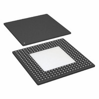
BSC A1 TOP 1.27 1.00 0.80 0.60 0.70 0.60 0.50 0.20 COPLANARITY REV. A OUTLINE DIMENSIONS 256-Ball Grid Array [SBGA] (BP-256) Dimensions shown in millimeters 1.27 24.13 REF 27.00 BSC 24.13 ...
Page 32
AD8152 Revision History Location 1/03—Data Sheet changed from REV REV. A. Edits to SPECIFICATIONS . . . . . . . . . . . . . . . . . . . . . . . . ...