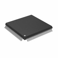
AD8191ASTZ Analog Devices Inc, AD8191ASTZ Datasheet - Page 17

AD8191ASTZ
Manufacturer Part Number
AD8191ASTZ
Description
IC,Telecom Switching Circuit,QFP,100PIN,PLASTIC
Manufacturer
Analog Devices Inc
Datasheet
1.AD8191ASTZ-RL.pdf
(32 pages)
Specifications of AD8191ASTZ
Function
Switch
Circuit
1 x 4:1
On-state Resistance
100 Ohm
Voltage Supply Source
Single Supply
Voltage - Supply, Single/dual (±)
3 V ~ 3.6 V
Operating Temperature
-40°C ~ 85°C
Mounting Type
Surface Mount
Package / Case
100-LQFP
Lead Free Status / RoHS Status
Lead free / RoHS Compliant
Available stocks
Company
Part Number
Manufacturer
Quantity
Price
Company:
Part Number:
AD8191ASTZ
Manufacturer:
ADI
Quantity:
180
Company:
Part Number:
AD8191ASTZ
Manufacturer:
Analog Devices Inc
Quantity:
10 000
Part Number:
AD8191ASTZ
Manufacturer:
ADI/亚德诺
Quantity:
20 000
Company:
Part Number:
AD8191ASTZ-RL
Manufacturer:
Analog Devices Inc
Quantity:
10 000
Company:
Part Number:
AD8191ASTZ/XST
Manufacturer:
ADI
Quantity:
210
GENERAL CASE
READ PROCEDURE
To read data from the AD8191 register set, an I
as a microcontroller) needs to send the appropriate control
signals to the AD8191 slave device. The signals are controlled
by the I
the procedure, see Figure 30. The steps for a read procedure are
as follows:
1.
2.
3.
4.
5.
6.
7.
8.
Send a start condition (while holding the I2C_SCL line
high, pull the I2C_SDA line low).
Send the AD8191 part address (seven bits). The upper four
bits of the AD8191 part address are the static value [1001]
and the three LSBs are set by Input Pin I2C_ADDR2, Input
Pin I2C_ADDR1, and Input Pin I2C_ADDR0 (LSB). This
transfer should be MSB first.
Send the write indicator bit (0).
Wait for the AD8191 to acknowledge the request.
Send the register address (eight bits) from which data is to
be read. This transfer should be MSB first.
Wait for the AD8191 to acknowledge the request.
Send a repeated start condition (Sr) by holding the
I2C_SCL line high and pulling the I2C_SDA line low.
The upper four bits of the AD8191 part address are the
static value [1001] and the three LSBs are set by the Input
Pin I2C_ADDR2, I2C_ADDR1 and Input Pin I2C_ADDR0
(LSB). This transfer should be MSB first.
EXAMPLE
Resend the AD8191 part address (seven bits) from Step 2.
I2C_SDA
I2C_SDA
I2C_SCL
2
C master, unless otherwise specified. For a diagram of
START
1
FIXED PART
2
ADDR
ADDR
R/W
3
ACK
4
2
5
C master (such
REGISTER ADDR
Figure 30. I
Rev. 0 | Page 17 of 32
2
C Read Diagram
ACK
6
7
SR
9.
10. Wait for the AD8191 to acknowledge the request.
11. The AD8191 serially transfers the data (eight bits) held in
12. Acknowledge the data from the AD8191.
13. Perform one of the following:
FIXED PART
the register indicated by the address set in Step 5. This data
is sent MSB first.
13a. S
13b.
13c.
13d.
Send the read indicator bit (1).
8
ADDR
line high, pull the SDA line high) and release control
of the bus to end the transaction (shown in
Send a repe
I2C_SCL line high, pull the I2C_SDA line low) and
continue with Step 2 of the write procedure (previous
Write Procedure section) to perform a write.
Send a repeated start condition (while holding the
I2C_SCL line high, pull the I2C_SDA line low) and
continue with Step 2 of this procedure to perform a
read from another address.
Send a repeated start conditi
I2C_SCL line high, pull the I2C_SDA line low) and
continue with Step 8 of this procedure to perform a
read from the same address.
end a st
ADDR
op condition (while holding the I2C_SCL
ated start condition (while holding the
R/W
9 10 11
ACK
on (while holding the
DATA
ACK
12
AD8191
Figure 30
STOP
13
).


