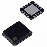
AD8290ACPZ-RL Analog Devices Inc, AD8290ACPZ-RL Datasheet - Page 14

AD8290ACPZ-RL
Manufacturer Part Number
AD8290ACPZ-RL
Description
IC,Sense Amplifier,SINGLE,CMOS,LLCC,16PIN,PLASTIC
Manufacturer
Analog Devices Inc
Datasheet
1.AD8290ACPZ-RL.pdf
(20 pages)
Specifications of AD8290ACPZ-RL
Amplifier Type
Current Sense
Number Of Circuits
1
-3db Bandwidth
250Hz
Current - Input Bias
100pA
Current - Supply
1.2mA
Voltage - Supply, Single/dual (±)
2.6 V ~ 5.5 V, ±1.3 V ~ 2.75 V
Operating Temperature
-40°C ~ 85°C
Mounting Type
Surface Mount
Package / Case
16-LFCSP
Lead Free Status / RoHS Status
Lead free / RoHS Compliant
Output Type
-
Current - Output / Channel
-
Slew Rate
-
Gain Bandwidth Product
-
Voltage - Input Offset
-
Lead Free Status / RoHS Status
Lead free / RoHS Compliant
AD8290
THEORY OF OPERATION
AMPLIFIER
The amplifier of the AD8290 is a precision current-mode
correction instrumentation amplifier. It is internally set to a
fixed gain of 50. The current-mode correction topology results
in excellent accuracy.
Figure 43 shows a simplified diagram illustrating the basic
operation of the instrumentation amplifier within the AD8290
(without correction). The circuit consists of a voltage-to-current
amplifier (M1 to M6), followed by a current-to-voltage amplifier
(R2 and A1). Application of a differential input voltage forces a
current through R1, resulting in a conversion of the input
voltage to a signal current. Transistors M3 to M6 transfer twice
the signal current to the inverting input of the op amp, A1. A1
and R2 form a current-to-voltage converter to produce a rail-to-
rail output voltage, V
Op Amp A1 is a high precision auto-zero amplifier. This
amplifier preserves the performance of the autocorrecting,
current-mode amplifier topology while offering the user a true
voltage-in, voltage-out instrumentation amplifier. Offset errors
are corrected internally.
An internal 0.9 V reference voltage is applied to the noninverting
input of A1 to set the output offset level. External Capacitor
C
FILTER
is used to filter out correction noise.
VINP
EXTERNAL
OUT
2I
I
.
M1
I
R1
=
(V
V
CC
R1
INP
Figure 43. Simplified Schematic of the Instrumentation Amplifier Within the AD8290
R1
– V
INN
)
2I
M2
I
VINN
M5
M3
I – I
R1
M4
Rev. B | Page 14 of 20
M6
I + I
I – I
V
BIAS
R1
R1
2I
R1
HIGH POWER SUPPLY REJECTION (PSR) AND
COMMON-MODE REJECTION (CMR)
PSR and CMR indicate the amount that the offset voltage of an
amplifier changes when its common-mode input voltage or power
supply voltage changes. The autocorrection architecture of the
AD8290 continuously corrects for offset errors, including those
induced by changes in input or supply voltage, resulting in
exceptional rejection performance. The continuous autocorrection
provides great CMR and PSR performances over the entire
operating temperature range (−40°C to +85°C).
1/f NOISE CORRECTION
Flicker noise, also known as 1/f noise, is noise inherent in the
physics of semiconductor devices and decreases 10 dB per decade.
The 1/f corner frequency of an amplifier is the frequency at which
the flicker noise is equal to the broadband noise of the amplifier. At
lower frequencies, flicker noise dominates causing large errors
in low frequency or dc applications.
Flicker noise appears as a slowly varying offset error that is
reduced by the autocorrection topology of the AD8290, allowing
the AD8290 to have lower noise near dc than standard low
noise instrumentation amplifiers.
V
C
REF
FILTER
R2
A1
= 0.9V
R3
V
OUT
= V
REF
+
2R2
R1
V
INP
– V
INN


