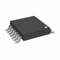
AD8302ARU-REEL7 Analog Devices Inc, AD8302ARU-REEL7 Datasheet - Page 17

AD8302ARU-REEL7
Manufacturer Part Number
AD8302ARU-REEL7
Description
IC,Phase/Frequency Detector,BIPOLAR,TSSOP,14PIN,PLASTIC
Manufacturer
Analog Devices Inc
Datasheet
1.AD8302ARUZ.pdf
(24 pages)
Specifications of AD8302ARU-REEL7
Rohs Status
RoHS non-compliant
Frequency
2.7GHz
Rf Type
General Purpose
Input Range
-60dBm ~ 0dBm
Accuracy
0.5dB
Voltage - Supply
2.7 V ~ 5.5 V
Current - Supply
23mA
Package / Case
14-TSSOP (0.173", 4.40mm Width)
Pin Count
14
Screening Level
Industrial
Package Type
TSSOP
Lead Free Status / Rohs Status
Not Compliant
Available stocks
Company
Part Number
Manufacturer
Quantity
Price
Part Number:
AD8302ARU-REEL7
Manufacturer:
ADI/亚德诺
Quantity:
20 000
Interfacing to the Input Channels
The single-ended input interfaces for both channels are identical.
Each consists of a driving pin, INPA and INPB, and an ac-
grounding pin, OFSA and OFSB. All four pins are internally
dc-biased at about 100 mV from the positive supply and should
be externally ac-coupled to the input signals and to ground. For
the signal pins, the coupling capacitor should offer negligible
impedance at the signal frequency. For the grounding pins, the
coupling capacitor has two functions: It provides ac grounding
and sets the high-pass corner frequency for the internal offset
compensation loop. There is an internal 10 pF capacitor to ground
that sets the maximum corner to approximately 200 MHz.
The corner can be lowered according the formula f
2/C
to ground, including the internal 10 pF.
The input impedance to INPA and INPB is a function of
frequency, the offset compensation capacitor, and package
parasitics. At moderate frequencies above f
can be approximated by a shunt 3 kΩ resistor in parallel with a
2 pF capacitor. At higher frequencies, the shunt resistance
decreases to approximately 500 Ω. The Smith Chart in Figure 6
shows the input impedance over the frequency range 100 MHz
to 3 GHz.
Figure 6. Smith Chart Showing the Input Impedance of a
Single Channel from 100 MHz to 3 GHz
A broadband resistive termination on the signal side of the coupling
capacitors can be used to match to a given source impedance.
The value of the termination resistor, R
where R
At higher frequencies, a reactive, narrow-band match might be
desirable to tune out the reactive portion of the input impedance.
An important attribute of the two-log-amp architecture is that if
both channels are at the same frequency and have the same input
network, then impedance mismatches and reflection losses become
essentially common-mode and hence do not impact the relative
gain and phase measurement. However, mismatches in these
external components can result in measurement errors.
REV. A
C
(nF), where C
R
T
IN
=
R R
is the input resistance and R
IN S
/
C
(
R
is the total capacitance from OFSA or OFSB
IN
3.0GHz
−
R
2.7GHz
S
)
2.2GHz
T
1.8GHz
, is determined by:
S
the source impedance.
900MHz
100MHz
HP
, the input network
HP
(MHz) =
(10)
–17–
Dynamic Range
The maximum measurement range for the gain subsystem is lim-
ited to a total of 60 dB distributed from –30 dB to +30 dB. This
means that both gain and attenuation can be measured. The limits
are determined by the minimum and maximum levels that each
individual log amp can detect. In the AD8302, each log amp can
detect inputs ranging from –73 dBV [(223 µV, –60 dBm re: 50 Ω
to –13 dBV (223 mV, 0 dBm re: 50 Ω)]. Note that log
amps respond to voltages and not power. An equivalent power
can be inferred given an impedance level, e.g., to convert from
dBV to dBm in a 50 Ω system, simply add 13 dB. To cover
the entire range, it is necessary to apply a reference level to one log
amp that corresponds precisely to its midrange. In the AD8302,
this level is at –43 dBV, which corresponds to –30 dBm in a 50 Ω
environment. The other channel can now sweep from its low end,
30 dB below midrange, to its high end, 30 dB above midrange. If
the reference is displaced from midrange, some measurement
range will be lost at the extremes. This can occur either if the log
amps run out of range or if the rails at ground or 1.8 V are reached.
Figure 7 illustrates the effect of the reference channel level placement.
If the reference is chosen lower than midrange by 10 dB, then the
lower limit will be at –20 dB rather than –30 dB. If the reference chosen
is higher by 10 dB, the upper limit will be 20 dB rather than 30 dB.
Figure 7. The Effect of Offsetting the Reference Level Is to
Reduce the Maximum Dynamic Range
The phase measurement range is of 0° to 180°. For phase differ-
ences of 0° to –180°, the transfer characteristics are mirrored as
shown in Figure 5, with a slope of the opposite sign. The phase
detector responds to the relative position of the zero crossings
between the two input channels. At higher frequencies, the finite
rise and fall times of the amplitude limited inputs create an
ambiguous situation that leads to inaccessible dead zones at the
0° and 180° limits. For maximum phase difference coverage, the
reference phase difference should be set to 90°.
1.80
0.90
–30
V
REF
< V
MAX RANGE FOR V
REF
GAIN MEASUREMENT RANGE – dB
OPT
0
REF
= V
REF
OPT
V
REF
> V
AD8302
REF
+30
OPT


