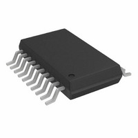
AD8331ARQZ-RL Analog Devices Inc, AD8331ARQZ-RL Datasheet - Page 7

AD8331ARQZ-RL
Manufacturer Part Number
AD8331ARQZ-RL
Description
IC,Voltage Controlled Gain Amplifier,SINGLE,SSOP,20PIN,PLASTIC
Manufacturer
Analog Devices Inc
Series
X-AMP®r
Type
Variable Gain Amplifierr
Datasheet
1.AD8331ARQZ.pdf
(56 pages)
Specifications of AD8331ARQZ-RL
Design Resources
Interfacing the High Frequency AD8331 to AD9215 (CN0096)
Applications
Signal Processing
Mounting Type
Surface Mount
Package / Case
20-QSOP
Lead Free Status / RoHS Status
Lead free / RoHS Compliant
ABSOLUTE MAXIMUM RATINGS
Table 2.
Parameter
Voltage
Power Dissipation
Temperature
θ
1
2
3
4-layer JEDEC board (2S2P).
Exposed pad soldered to board, nine thermal vias in pad—JEDEC, 4-layer
board J-STD-51-9.
Exposed pad soldered to board, 25 thermal vias in pad—JEDEC, 4-layer
board J-STD-51-9.
JA
Supply Voltage (VPSn, VPSV, VPSL, VPOS)
Input Voltage (INHx)
ENB, ENBL, ENBV, HILO Voltage
GAIN Voltage
RU Package
CP-32 Package (AD8332)
RQ Package
CP-64 Package (AD8334)
Operating Temperature Range
Storage Temperature Range
Lead Temperature (Soldering 60 sec)
RU Package
CP-32 Package2
RQ Package
CP-64 Package
1
1
1
1
(AD8332)
(AD8331)
(AD8331)
(AD8332)
3
2
(AD8334)
(AD8332)
Rating
5.5 V
V
2.5 V
1.97 W
0.91 W
−40°C to +85°C
V
0.96 W
0.78 W
−65°C to +150°C
300°C
68°C/W
33°C/W
83°C/W
24.2°C/W
S
S
+ 200 mV
+ 200 mV
Rev. G | Page 7 of 56
Stresses above those listed under Absolute Maximum Ratings
may cause permanent damage to the device. This is a stress
rating only; functional operation of the device at these or any
other conditions above those indicated in the operational
section of this specification is not implied. Exposure to absolute
maximum rating conditions for extended periods may affect
device reliability.
ESD CAUTION
AD8331/AD8332/AD8334


