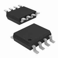
AD8350AR20 Analog Devices Inc, AD8350AR20 Datasheet - Page 8

AD8350AR20
Manufacturer Part Number
AD8350AR20
Description
Buffer Amplifier IC
Manufacturer
Analog Devices Inc
Datasheet
1.AD8350ARZ20-REEL7.pdf
(16 pages)
Specifications of AD8350AR20
Bandwidth
900MHz
Mounting Type
Surface Mount
Package / Case
8-SOIC
Rohs Status
RoHS non-compliant
Current - Supply
28mA
Frequency
0Hz ~ 1GHz
Gain
20dB
Noise Figure
5.9dB
Rf Type
CATV
Test Frequency
250MHz
Voltage - Supply
5 V ~ 10 V
P1db
-
Lead Free Status / RoHS Status
Available stocks
Company
Part Number
Manufacturer
Quantity
Price
Part Number:
AD8350AR20
Manufacturer:
ADI/亚德诺
Quantity:
20 000
Part Number:
AD8350AR20-REEL
Manufacturer:
ADI/亚德诺
Quantity:
20 000
Part Number:
AD8350AR20-REEL7
Manufacturer:
ADI/亚德诺
Quantity:
20 000
Company:
Part Number:
AD8350AR20REEL
Manufacturer:
PH
Quantity:
3 256
APPLICATIONS
Using the AD8350
Figure 1 shows the basic connections for operating the AD8350.
A single supply in the range 5 V to 10 V is required. The power
supply pin should be decoupled using a 0.1 µF capacitor. The
ENBL pin is tied to the positive supply or to 5 V (when V
10 V) for normal operation and should be pulled to ground to
put the device in sleep mode. Both the inputs and the outputs
have dc bias levels at midsupply and should be ac-coupled.
Also shown in Figure 1 are the impedance balancing requirements,
either resistive or reactive, of the input and output. With an
input and output impedance of 200 Ω, the AD8350 should be
driven by a 200 Ω source and loaded by a 200 Ω impedance. A
reactive match can also be implemented.
Figure 2 shows how the AD8350 can be driven by a single-
ended source. The unused input should be ac-coupled to ground.
When driven single-endedly, there will be a slight imbalance in
the differential output voltages. This will cause an increase in
the second order harmonic distortion (at 50 MHz, with V
10 V and V
harmonic on AD8350-15).
Reactive Matching
In practical applications, the AD8350 will most likely be matched
using reactive matching components as shown in Figure 3.
Matching components can be calculated using a Smith Chart or
by using a resonant approach to determine the matching network
that results in a complex conjugate match. In either situation,
the circuit can be analyzed as a single-ended equivalent circuit
to ease calculations as shown in Figure 4.
AD8350
SOURCE
SOURCE
Z = 100
Z = 100
Z = 200
OUT
= 1 V p-p, –59 dBc was measured for the second
0.001 F
0.001 F
0.001 F
0.001 F
C2
C1
ENBL (5V)
ENBL (5V)
C2
C1
8
1
8
1
+V
+V
AD8350
AD8350
–
–
7
2
7
2
S
S
(5V TO 10V)
(5V TO 10V)
6
3
6
3
5
4
5
4
C5
0.1 F
C5
0.1 F
0.001 F
0.001 F
0.001 F
0.001 F
C3
C3
C4
C4
Z = 200
Z = 200
LOAD
CC
CC
LOAD
=
=
When the source impedance is smaller than the load impedance,
a step-up matching network is required. A typical step-up network
is shown on the input of the AD8350 in Figure 3. For purely
resistive source and load impedances the resonant approach may
be used. The input and output impedance of the AD8350 can be
modeled as a real 200 Ω resistance for operating frequencies less
than 100 MHz. For signal frequencies exceeding 100 MHz, classi-
cal Smith Chart matching techniques should be invoked in order
to deal with the complex impedance relationships. Detailed S
parameter data measured differentially in a 200 Ω system can be
found in Tables II and III.
For the input matching network the source resistance is less
than the input resistance of the AD8350. The AD8350 has a
nominal 200 Ω input resistance from Pins 1 to 8. The reactance
of the ac-coupling capacitors, C
capacitors are used and the lowest signal frequency is greater
than 1 MHz. If the series reactance of the matching network
inductor is defined to be X
of the matching capacitor to be X
For a 70 MHz application with a 50 Ω source resistance, and
assuming the input impedance is 200 Ω, or R
then X
ing component values:
R
R
V
V
R
S
S
S
S
/2
/2
S
X
S
=
P
C
= 115.5 Ω and X
L
L
R
L
S
S
P
S
/2
/2
S
L
= (2 π × 70 × 10
×
S
C
C
X
P
P
= 86.6 × (2 π × 70 × 10
R
P
LOAD
ENBL (5V)
ENBL (5V)
C
C
C
C
AC
AC
AC
AC
where
S
8
1
8
1
S
= 86.6 Ω, which results in the follow-
+V
+V
AD8350
AD8350
= 2 π f L
6
X
–
–
7
2
7
2
S
S
× 115.5)
AC
(5V TO 10V)
P
(5V TO 10V)
, should be negligible if 100 nF
=
6
3
6
3
P
R
= (2 π f C
LOAD
5
4
5
4
0.1 F
0.1 F
S
, and the shunt reactance
6
–1
)
–1
C
C
C
C
= 19.7 pF and
AC
AC
AC
AC
×
= 197 nH
LOAD
P
R
)
–1
LOAD
C
C
, then:
= R
P
P
R
L
L
S
L
IN
S
–
S
S
/2
/2
R
= 200 Ω,
S
R
R
LOAD
LOAD
(1)


