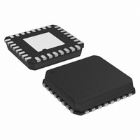
AD8376ACPZ-R7 Analog Devices Inc, AD8376ACPZ-R7 Datasheet

AD8376ACPZ-R7
Specifications of AD8376ACPZ-R7
Available stocks
Related parts for AD8376ACPZ-R7
AD8376ACPZ-R7 Summary of contents
Page 1
FEATURES Dual independent digitally controlled VGAs Bandwidth of 700 MHz (−3 dB) Gain range: − +20 dB Step size ± 0.2 dB Differential input and output Noise figure: 8 maximum gain Output IP3 of ...
Page 2
AD8376 TABLE OF CONTENTS Features .............................................................................................. 1 Applications....................................................................................... 1 Functional Block Diagram .............................................................. 1 General Description ......................................................................... 1 Revision History ............................................................................... 2 Specifications..................................................................................... 3 Absolute Maximum Ratings............................................................ 5 ESD Caution.................................................................................. 5 Pin Configuration and Function Descriptions............................. 6 Typical Performance Characteristics ...
Page 3
SPECIFICATIONS 25° 150 Ω at 140 MHz p-p differential output, both channels enabled, unless otherwise noted Table 1. Parameter DYNAMIC PERFORMANCE −3 dB Bandwidth Slew ...
Page 4
AD8376 Parameter POWER INTERFACE Supply Voltage VCC and Output Quiescent Current with Both Channels Enabled vs. Temperature Power-Down Current, Both Channels vs. Temperature POWER-UP/GAIN CONTROL Logic Input Bias Current Table 2. Gain Code vs. Voltage Gain ...
Page 5
ABSOLUTE MAXIMUM RATINGS Table 3. Parameter Supply Voltage, V POS ENBA, ENBB A4 Input Voltage IN+ IN− DC Common Mode VCMA, VCMB Internal Power Dissipation θ (Exposed Paddle Soldered Down) JA θ ...
Page 6
AD8376 PIN CONFIGURATION AND FUNCTION DESCRIPTIONS Table 4. Pin Function Descriptions Pin No. Mnemonic Description 1 A2 MSB − 2 for the Gain Control Interface for Channel MSB − 1 for the Gain Control Interface for Channel ...
Page 7
TYPICAL PERFORMANCE CHARACTERISTICS 25° 150 Ω p-p output, maximum gain unless otherwise noted 46MHz, +5V 70MHz, +5V 20 140MHz, + ...
Page 8
AD8376 +20dB +10dB 0dB –4dB 110 130 FREQUENCY (MHz) Figure 10. ...
Page 9
HD2 –4dB HD2 0dB –80 HD2 +10dB HD2 +20dB –85 –90 –95 HD3 –4dB HD3 0dB –100 HD3 +10dB HD3 +20dB –105 –110 –115 100 120 140 160 FREQUENCY (MHz) Figure 16. Harmonic Distortion vs. Frequency ...
Page 10
AD8376 2 1 CH1 500mV Ω CH2 500mV Ω M10.0ns 10.0GS/s IT 10.0ps/pt A CH1 Figure 22. Gain Step Time Domain Response 2 1 CH1 500mV Ω CH2 500mV Ω M20.0ns 10.0GS/s IT 20.0ps/pt A CH1 Figure 23. ENBL Time ...
Page 11
FREQUENCY (MHz) Figure 28. Reverse Isolation vs. Frequency 0 –10 –20 –30 –40 –50 –60 –70 –80 –90 –100 10 100 FREQUENCY (MHz) Figure 29. ...
Page 12
AD8376 CIRCUIT DESCRIPTION BASIC STRUCTURE The AD8376 is a dual differential variable gain amplifier with each amplifier consisting of a 150 Ω digitally controlled passive attenuator followed by a highly linear transconductance amplifier. 1/2 AD8376 ATTENUATOR MUX BUFFERS IP+ VCM ...
Page 13
APPLICATIONS BASIC CONNECTIONS Figure 36 shows the basic connections for operating the AD8376. A voltage between 4.5 V and 5.5 V should be applied to the supply pins. Each supply pin should be decoupled with at least one low inductance, ...
Page 14
AD8376 CHANNEL A PARALLEL CONTROL INTERFACE 0.1µF 4 VCMA 5 VCMB 0.1µ CHANNEL B PARALLEL CONTROL INTERFACE BALANCED SOURCE ...
Page 15
BROADBAND OPERATION The AD8376 uses an open-collector output structure that requires dc bias through an external bias network. Typically, choke inductors are used to provide bias to the open-collector outputs. Choke inductors work well at signal frequencies where the impedance ...
Page 16
AD8376 For optimum performance, the AD8376 should be driven differentially using an input balun or impedance transformer. Figure 39 uses a wideband 1:1 transmission line balun followed by two 37.5 Ω resistors in parallel with the 150 Ω input imped- ...
Page 17
Figure 42 is optimized for driving some of Analog Devices popular unbuffered ADCs, such as the AD9246, AD9640, and AD6655. Table 5 includes antialiasing filter component recommendations for popular IF sampling center frequencies. Inductor L5 works in parallel with the ...
Page 18
AD8376 LAYOUT CONSIDERATIONS Each amplifier has two output pins for each polarity, and they are oriented in an alternating fashion. When designing the board, care should be taken to minimize the parasitic capaci- tance due to the routing that connects ...
Page 19
EVALUATION BOARD Figure 47 shows the schematic of the AD8376 evaluation board. The silkscreen and layout of the component and circuit sides are shown in Figure 48 through Figure 51. The board is powered by a single supply in the ...
Page 20
AD8376 Figure 47. AD8376 Evaluation Board Schematic Rev Page ...
Page 21
Table 6. Evaluation Board Configuration Options Components Function C13, C14, C20 to C22, Power Supply Decoupling. Nominal supply decoupling consists a C64 to C67, R90, R91 10 μF capacitor to ground followed by 0.1 μF capacitors to ground positioned as ...
Page 22
AD8376 \ Figure 48. Component Side Silkscreen Figure 49. Circuit Side Silkscreen Figure 50. Component Side Layout Figure 51. Circuit Side Layout Rev Page ...
Page 23
... OUTLINE DIMENSIONS PIN 1 INDICATOR 12° MAX 1.00 0.85 0.80 SEATING PLANE ORDERING GUIDE 1 Model Temperature Range AD8376ACPZ-WP −40°C to +85°C AD8376ACPZ-R7 −40°C to +85°C AD8376-EVALZ RoHS Compliant Part. 5.00 BSC SQ 0.60 MAX 24 0.50 BSC TOP 4.75 VIEW BSC SQ 0.50 ...
Page 24
AD8376 NOTES ©2007–2010 Analog Devices, Inc. All rights reserved. Trademarks and registered trademarks are the property of their respective owners. D06725-0-10/10(A) Rev Page ...


