AD9219-65EBZ Analog Devices Inc, AD9219-65EBZ Datasheet - Page 19
AD9219-65EBZ
Manufacturer Part Number
AD9219-65EBZ
Description
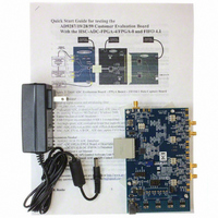
Quad 10-bit 65 MSPS Serial LVDS ADC EB
Manufacturer
Analog Devices Inc
Datasheet
1.AD9219ABCPZRL7-40.pdf
(52 pages)
Specifications of AD9219-65EBZ
Number Of Adc's
4
Number Of Bits
10
Sampling Rate (per Second)
40M
Data Interface
Serial
Inputs Per Adc
2 Single
Input Range
2 Vpp
Power (typ) @ Conditions
378mW @ 1.8 V
Voltage Supply Source
Single Supply
Operating Temperature
-40°C ~ 85°C
Utilized Ic / Part
AD9219
Lead Free Status / RoHS Status
Lead free / RoHS Compliant


THEORY OF OPERATION
The AD9219 architecture consists of a pipelined ADC divided into
three sections: a 4-bit first stage followed by eight 1.5-bit stages and
a final 3-bit flash. Each stage provides sufficient overlap to correct
for flash errors in the preceding stage. The quantized outputs from
each stage are combined into a final 10-bit result in the digital
correction logic. The pipelined architecture permits the first stage
to operate with a new input sample while the remaining stages
operate with preceding samples. Sampling occurs on the rising
edge of the clock.
Each stage of the pipeline, excluding the last, consists of a low
resolution flash ADC connected to a switched-capacitor DAC
and an interstage residue amplifier (for example, a multiplying
digital-to-analog converter (MDAC)). The residue amplifier
magnifies the difference between the reconstructed DAC output
and the flash input for the next stage in the pipeline. One bit of
redundancy is used in each stage to facilitate digital correction of
flash errors. The last stage simply consists of a flash ADC.
The output staging block aligns the data, corrects errors, and
passes the data to the output buffers. The data is then serialized
and aligned to the frame and data clocks.
ANALOG INPUT CONSIDERATIONS
The analog input to the AD9219 is a differential switched-
capacitor circuit designed for processing differential input
signals. This circuit can support a wide common-mode range
while maintaining excellent performance. By using an input
common-mode voltage of midsupply, users can minimize
signal-dependent errors and achieve optimum performance.
VIN + x
VIN – x
Figure 43. Switched-Capacitor Input Circuit
C
C
PAR
PAR
H
H
S
S
C
C
SAMPLE
SAMPLE
S
S
H
H
Rev. D | Page 19 of 52
The clock signal alternately switches the input circuit between
sample mode and hold mode (see Figure 43). When the input
circuit is switched to sample mode, the signal source must be
capable of charging the sample capacitors and settling within
one-half of a clock cycle. A small resistor in series with each
input can help reduce the peak transient current injected from
the output stage of the driving source. In addition, low-Q inductors
or ferrite beads can be placed on each leg of the input to reduce
high differential capacitance at the analog inputs and therefore
achieve the maximum bandwidth of the ADC. Such use of low-
Q inductors or ferrite beads is required when driving the converter
front end at high IF frequencies. Either a shunt capacitor or two
single-ended capacitors can be placed on the inputs to provide a
matching passive network. This ultimately creates a low-pass
filter at the input to limit unwanted broadband noise. See the
AN-742 Application Note, the AN-827 Application Note, and the
Analog Dialogue article “Transformer-Coupled Front-End for
Wideband A/D Converters” (Volume 39, April 2005) for more
information at www.analog.com. In general, the precise values
depend on the application.
The analog inputs of the AD9219 are not internally dc-biased.
Therefore, in ac-coupled applications, the user must provide
this bias externally. Setting the device so that V
recommended for optimum performance, but the device can
function over a wider range with reasonable performance, as
shown in Figure 44 to Figure 47.
CM
= AVDD/2 is
AD9219
Related parts for AD9219-65EBZ
Image
Part Number
Description
Manufacturer
Datasheet
Request
R

Part Number:
Description:
Quad 10-bit 65 MSPS Serial LVDS ADC EB
Manufacturer:
Analog Devices Inc
Datasheet:

Part Number:
Description:
±1.7g Dual-Axis IMEMS Accelerometer Evaluation Board
Manufacturer:
Analog Devices Inc
Datasheet:
Part Number:
Description:
Inertial Sensor Evaluation System
Manufacturer:
Analog Devices Inc
Datasheet:
Part Number:
Description:
Manufacturer:
Analog Devices Inc
Datasheet:
Part Number:
Description:
Manufacturer:
Analog Devices Inc
Datasheet:
Part Number:
Description:
Manufacturer:
Analog Devices Inc
Datasheet:
Part Number:
Description:
Manufacturer:
Analog Devices Inc
Datasheet:
Part Number:
Description:
Manufacturer:
Analog Devices Inc
Datasheet:
Part Number:
Description:
Manufacturer:
Analog Devices Inc
Datasheet:
Part Number:
Description:
Manufacturer:
Analog Devices Inc
Datasheet:
Part Number:
Description:
Manufacturer:
Analog Devices Inc
Datasheet:
Part Number:
Description:
Manufacturer:
Analog Devices Inc
Datasheet:
Part Number:
Description:
Manufacturer:
Analog Devices Inc
Datasheet: