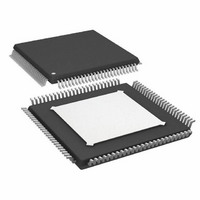
AD9273BSVZ-40 Analog Devices Inc, AD9273BSVZ-40 Datasheet - Page 27

AD9273BSVZ-40
Manufacturer Part Number
AD9273BSVZ-40
Description
12Bit 40 MSPS Octal ADC
Manufacturer
Analog Devices Inc
Type
Crosspoint Switchr
Datasheet
1.AD9273BSVZ-25.pdf
(48 pages)
Specifications of AD9273BSVZ-40
Resolution (bits)
12 b
Sampling Rate (per Second)
40M
Data Interface
Serial
Voltage Supply Source
Single Supply
Voltage - Supply
1.7 V ~ 3.6 V
Operating Temperature
-40°C ~ 85°C
Mounting Type
Surface Mount
Package / Case
100-TQFP Exposed Pad, 100-eTQFP, 100-HTQFP, 100-VQFP
Lead Free Status / RoHS Status
Lead free / RoHS Compliant
Available stocks
Company
Part Number
Manufacturer
Quantity
Price
Company:
Part Number:
AD9273BSVZ-40
Manufacturer:
Analog Devices Inc
Quantity:
10 000
Part Number:
AD9273BSVZ-40
Manufacturer:
ADI/亚德诺
Quantity:
20 000
Crosspoint Switch
Each LNA is followed by a transconductance amp for voltage-
to-current conversion. Currents can be routed to one of eight
pairs of differential outputs or to 16 single-ended outputs for
summing. Each CWD output pin sinks 2.4 mA dc current, and
the signal has a full-scale current of ±2 mA for each channel
selected by the crosspoint switch. For example, if four channels
are summed on one CWD output, the output sinks 9.6 mA dc
and has a full-scale current output of ±8 mA.
The maximum number of channels combined must be considered
when setting the load impedance for current-to-voltage conversion
to ensure that the full-scale swing and common-mode voltage
are within the operating limits of the AD9273. When interfacing
to the AD8339, a common-mode voltage of 2.5 V and a full-scale
swing of 2.8 V p-p are desired. This can be accomplished by
connecting an inductor between each CWD output and a 2.5 V
supply, and then connecting either a single-ended or differential
load resistance to the CWDx± outputs. The value of resistance
should be calculated based on the maximum number of channels
that can be combined.
CWDx± outputs are required under full-scale swing to be
greater than 1.5 V and less than AVDD2 (3.0 V supply).
TGC OPERATION
The TGC signal path is fully differential throughout to maximize
signal swing and reduce even-order distortion; however, the LNAs
are designed to be driven from a single-ended signal source. Gain
values are referenced from the single-ended LNA input to the
differential ADC input. A simple exercise in understanding the
maximum and minimum gain requirements is shown in Figure 47.
(5.4µV rms) @ AAF BW = 15MHz
LNA + VGA NOISE = 1.4nV/ Hz
Figure 47. Gain Requirements of TGC Operation for a 12-Bit, 40 MSPS ADC
LNA INPUT-REFERRED
NOISE FLOOR
(0.55V p-p SE)
LNA
MINIMUM GAIN
LNA FS
91dB
VGA GAIN RANGE > 42dB
MAX CHANNEL GAIN > 48dB
MAXIMUM GAIN
70dB
>11dB MARGIN
ADC NOISE FLOOR
(224µV rms)
ADC FS (2V p-p)
~10dB MARGIN
ADC
Rev. B | Page 27 of 48
The maximum gain required is determined by
The minimum gain required is determined by
Therefore, 42 dB of gain range for a 12-bit, 40 MSPS ADC with
15 MHz of bandwidth should suffice in achieving the dynamic
range required for most of today’s ultrasound systems.
The system gain is distributed as listed in Table 8.
Table 8. Channel Gain Distribution
Section
LNA
Attenuator
VGA Amp
Filter
ADC
The linear-in-dB gain (law conformance) range of the TGC path
is 42 dB. The slope of the gain control interface is 28 dB/V, and
the gain control range is −0.8 V to +0.8 V. Equation 3 is the
expression for the differential voltage V
the expression for the channel gain.
where ICPT is the intercept point of the TGC gain.
In its default condition, the LNA has a gain of 21.3 dB (12×) and
the VGA postamp gain is 24 dB if the voltage on the GAIN+ pin is
0 V and the voltage on the GAIN− pin is 0.8 V (42 dB attenuation).
This gives rise to a total gain (or ICPT) of 3.6 dB through the
TGC path if the LNA input is unmatched, or of −2.4 dB if the
LNA is matched to 50 Ω (R
GAIN+ pin is 1.6 V and the voltage on the GAIN− pin is 0.8 V
(0 dB attenuation), however, the VGA gain is 24 dB. This results
in a total gain of 45 dB through the TGC path if the LNA input is
unmatched, or in a total gain of 39 dB if the LNA input is matched.
Each LNA output is dc-coupled to a VGA input. The VGA consists
of an attenuator with a range of −42 dB to 0 dB followed by an
amplifier with 21 dB, 24 dB, 27 dB, or 30 dB of gain. The X-AMP
gain-interpolation technique results in low gain error and uniform
bandwidth, and differential signal paths minimize distortion.
(ADC Noise Floor/VGA Input Noise Floor) + Margin =
(ADC Input FS/VGA Input FS) + Margin =
V
Gain
GAIN
20 log(224/5.4) + 11 dB = 43 dB
20 log(2/0.55) – 10 dB = 3 dB
(
(
dB
V
)
)
=
=
GAIN
28
dB
V
(
V
+
)
GAIN
Nominal Gain (dB)
15.6/17.9/21.3
−42 to 0
21/24/27/30
0
0
−
FB
GAIN
= 350 Ω). If the voltage on the
+
ICPT
(
−
)
GAIN
, and Equation 4 is
AD9273
(3)
(4)


