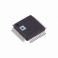
AD9288BSTZ-80 Analog Devices Inc, AD9288BSTZ-80 Datasheet - Page 14

AD9288BSTZ-80
Manufacturer Part Number
AD9288BSTZ-80
Description
IC,A/D CONVERTER,DUAL,8-BIT,CMOS,QFP,48PIN
Manufacturer
Analog Devices Inc
Datasheet
1.AD9288BSTZ-40.pdf
(24 pages)
Specifications of AD9288BSTZ-80
Number Of Bits
8
Sampling Rate (per Second)
80M
Data Interface
Parallel
Number Of Converters
2
Power Dissipation (max)
207mW
Voltage Supply Source
Analog and Digital
Operating Temperature
-40°C ~ 85°C
Mounting Type
Surface Mount
Package / Case
48-LQFP
Lead Free Status / RoHS Status
Lead free / RoHS Compliant
Available stocks
Company
Part Number
Manufacturer
Quantity
Price
Company:
Part Number:
AD9288BSTZ-80
Manufacturer:
AD
Quantity:
1
Company:
Part Number:
AD9288BSTZ-80
Manufacturer:
Analog Devices Inc
Quantity:
10 000
Part Number:
AD9288BSTZ-80
Manufacturer:
ADI/亚德诺
Quantity:
20 000
AD9288
THEORY OF OPERATION
The AD9288 ADC architecture is a bit-per-stage pipeline-type
converter utilizing switch capacitor techniques. These stages
determine the 5 MSBs and drive a 3-bit flash. Each stage
provides sufficient overlap and error correction, allowing
optimization of comparator accuracy. The input buffers are
differential, and both sets of inputs are internally biased. This
allows the most flexible use of ac or dc and differential or
single-ended input modes. The output staging block aligns the
data, carries out the error correction, and feeds the data to
output buffers. The set of output buffers are powered from a
separate supply, allowing adjustment of the output voltage
swing. There is no discernible difference in performance
between the two channels.
USING THE AD9288
Good high speed design practices must be followed when
using the AD9288. To obtain maximum benefit, decoupling
capacitors should be physically as close as possible to the chip,
minimizing trace and via inductance between chip pins and
capacitor (0603 surface-mount capacitors are used on the
AD9288/PCB evaluation board). It is recommended to place a
0.1 µF capacitor at each power-ground pin pair for high
frequency decoupling, and to include one 10 µF capacitor for
local low frequency decoupling. The VREF IN pin should also
be decoupled by a 0.1 µF capacitor. It is also recommended to
use a split power plane and a contiguous ground plane (see the
Evaluation Board section). Data output traces should be short
(< 1 inch), minimizing on-chip noise at switching.
ENCODE INPUT
Any high speed A/D converter is extremely sensitive to the
quality of the sampling clock provided by the user. A track-and-
hold circuit is essentially a mixer. Any noise, distortion, or
timing jitter on the clock is combined with the desired signal at
the A/D output. For that reason, considerable care has been
taken in the design of the Encode (Clock) input of the AD9288,
and the user is advised to give commensurate thought to the
clock source. The Encode input is fully TTL/CMOS-compatible.
DIGITAL OUTPUTS
The digital outputs are TTL/CMOS-compatible for lower power
consumption. During standby, the output buffers transition to a
high impedance state. A data format selection option supports
either twos complement (set high) or offset binary output (set
low) formats.
ANALOG INPUT
The analog input to the AD9288 is a differential buffer. For best
dynamic performance, impedance at A
Special care was taken in the design of the analog input stage of
the AD9288 to prevent damage and corruption of data when
IN
and A
IN
should match.
Rev. C | Page 14 of 24
the input is overdriven. The nominal input range is 1.024 V p-p
centered at V
VOLTAGE REFERENCE
A stable and accurate 1.25 V voltage reference is built into the
AD9288 (REF
is used by strapping Pins 5 (REF
(REFOUT). The input range can be adjusted by varying the
reference voltage applied to the AD9288. No appreciable
degradation in performance occurs when the reference is
adjusted ±5%. The full-scale range of the ADC tracks reference
voltage, which changes linearly.
TIMING
The AD9288 provides latched data outputs, with four pipeline
delays. Data outputs are available one propagation delay (t
after the rising edge of the Encode command (see Figure 2,
Figure 3, and Figure 4). The length of the output data lines and
loads placed on them must be minimized to reduce transients
within the AD9288. These transients can detract from the
converter’s dynamic performance.
The minimum guaranteed conversion rate of the AD9288 is
1 MSPS. At clock rates below 1 MSPS, dynamic performance
degrades. Typical power-up recovery time after standby mode is
15 clock cycles.
USER-SELECTABLE OPTIONS
Two pins are available for a combination of operational modes.
These options allow the user to place both channels, excluding
the reference, into standby mode, or just the B channel. Both
modes place the output buffers and clock inputs into high
impedance states.
The other option allows the user to skew the B channel output
data by 1/2 of a clock cycle. In other words, if two clocks are fed
to the AD9288 and are 180° out of phase, enabling the data
align allows Channel B output data to be available at the rising
edge of Clock A. If the same Encode clock is provided to both
channels and the data align pin is enabled, then output data
from Channel B is 180° out of phase with respect to Channel A.
If the same Encode clock is provided to both channels and the
data align pin is disabled, both outputs are delivered on the
same rising edge of the clock.
Table 4. User-Selectable Options
S1
0
0
1
1
S2
0
1
0
1
Option
Standby Both Channels A and B.
Standby Channel B Only.
Normal Operation (Data Align Disabled).
Data Align Enabled (data from both channels avail-
able on rising edge of Clock A. Channel B data is
delayed a 1/2 clock cycle).
D
OUT
× 0.3.
). In normal operation, the internal reference
IN
A) and 7 (REF
IN
B) to Pin 6
PD
)


