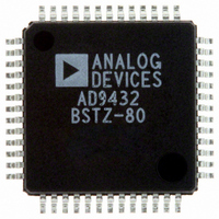
AD9432BSTZ-80 Analog Devices Inc, AD9432BSTZ-80 Datasheet - Page 13

AD9432BSTZ-80
Manufacturer Part Number
AD9432BSTZ-80
Description
IC,A/D CONVERTER,SINGLE,12-BIT,BICMOS,QFP,52PIN
Manufacturer
Analog Devices Inc
Datasheet
1.AD9432BSTZ-80.pdf
(16 pages)
Specifications of AD9432BSTZ-80
Number Of Bits
12
Sampling Rate (per Second)
80M
Data Interface
Parallel
Number Of Converters
1
Power Dissipation (max)
1W
Voltage Supply Source
Single Supply
Operating Temperature
-40°C ~ 85°C
Mounting Type
Surface Mount
Package / Case
52-LQFP Exposed Pad, 52-eLQFP, 52-HLQFP
Package
52LQFP
Resolution
12 Bit
Sampling Rate
80 MSPS
Architecture
Pipelined
Number Of Analog Inputs
1
Digital Interface Type
Parallel
Input Type
Voltage
Signal To Noise Ratio
67.5(Typ) dB
Polarity Of Input Voltage
Unipolar
Lead Free Status / RoHS Status
Lead free / RoHS Compliant
Available stocks
Company
Part Number
Manufacturer
Quantity
Price
Company:
Part Number:
AD9432BSTZ-80
Manufacturer:
Analog Devices Inc
Quantity:
10 000
THEORY OF OPERATION
The AD9432 is a 12-bit pipeline converter that uses a switched-
capacitor architecture. Optimized for high speed, this converter
provides flat dynamic performance up to frequencies near
Nyquist. DNL transitional errors are calibrated at final test to
a typical accuracy of 0.25 LSB or less.
ANALOG INPUT
The analog input to the AD9432 is a differential buffer. The
input buffer is self-biased by an on-chip resistor divider that
sets the dc common-mode voltage to a nominal 3 V (see the
Equivalent Circuits section). Rated performance is achieved
by driving the input differentially. The minimum input offset
voltage is obtained when driving from a source with a low
differential source impedance, such as a transformer in ac
applications. Capacitive coupling at the inputs increases the
input offset voltage by as much as ±25 mV. Driving the ADC
single-ended degrades performance. For best dynamic perfor-
mance, impedances at AIN and AIN should match.
Special care was taken in the design of the analog input section
of the AD9432 to prevent damage and corruption of data when
the input is overdriven. The nominal input range is 2 V p-p.
Each analog input is 1 V p-p when driven differentially.
ENCODE INPUT
Any high speed ADC is extremely sensitive to the quality of the
sampling clock provided by the user. A track-and-hold circuit is
essentially a mixer, and any noise, distortion, or timing jitter on
the clock is combined with the desired signal at the ADC output.
For this reason, considerable care has been taken in the design
of the encode input of the AD9432, and the user is advised to
give commensurate thought to the clock source. The encode
input supports differential or single-ended mode and is fully
TTL-/CMOS-compatible.
4.0
3.5
3.0
2.5
2.0
Figure 26. Full-Scale Analog Input Range
AIN
AIN
Rev. F | Page 13 of 16
Note that the encode inputs cannot be driven directly from PECL
level signals (V
easily be accommodated by ac coupling, as shown in Figure 27.
Good performance is obtained using an MC10EL16 translator
in the circuit to drive the encode inputs.
ENCODE VOLTAGE LEVEL DEFINITION
The voltage level definitions for driving ENCODE and ENCODE
in single-ended and differential mode are shown in
Table 5. Encode Inputs
Input
Differential Signal Amplitude (V
High Differential Input Voltage (V
Low Differential Input Voltage (V
Common-Mode Input (V
High Single-Ended Voltage (V
Low Single-Ended Voltage (V
Often, the cleanest clock source is a crystal oscillator producing a
pure sine wave. In this configuration, or with any roughly symmet-
rical clock input, the input can be ac-coupled and biased to a
reference voltage that also provides the encode. This ensures
that the reference voltage is centered on the encode signal.
ENCODE
ENCODE
ENCODE
0.1µF
GATE
PECL
Figure 28. Differential and Single-Ended Input Levels
510Ω
IHD
Figure 27. AC Coupling to Encode Inputs
is 3.5 V maximum). PECL level signals can
V
V
V
V
V
ICM
IHD
IHS
ILD
ILS
510Ω
ICM
)
ILS
IHS
0.1µF
0.1µF
)
IHD
ID
ILD
)
)
)
)
500 mV
0 V
Min
1.25 V
2 V
0 V
V
ID
ENCODE
ENCODE
AD9432
Nominal
750 mV
1.6 V
Figure 28
AD9432
Max
3.5 V
3.5 V
0.8 V
.


