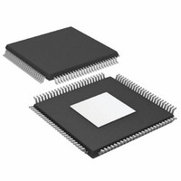
AD9776ABSVZRL Analog Devices Inc, AD9776ABSVZRL Datasheet - Page 50

AD9776ABSVZRL
Manufacturer Part Number
AD9776ABSVZRL
Description
IC,D/A CONVERTER,DUAL,12-BIT,CMOS,TQFP,100PIN
Manufacturer
Analog Devices Inc
Datasheet
1.AD9776ABSVZ.pdf
(60 pages)
Specifications of AD9776ABSVZRL
Number Of Bits
12
Data Interface
Parallel
Number Of Converters
2
Voltage Supply Source
Analog and Digital
Power Dissipation (max)
300mW
Operating Temperature
-40°C ~ 85°C
Mounting Type
Surface Mount
Package / Case
100-TQFP Exposed Pad, 100-eTQFP, 100-HTQFP, 100-VQFP
Lead Free Status / RoHS Status
Lead free / RoHS Compliant
For Use With
AD9776A-EBZ - BOARD EVALUATION AD9776A
Settling Time
-
Lead Free Status / RoHS Status
Lead free / RoHS Compliant
Available stocks
Company
Part Number
Manufacturer
Quantity
Price
Company:
Part Number:
AD9776ABSVZRL
Manufacturer:
Analog Devices Inc
Quantity:
10 000
AD9776A/AD9778A/AD9779A
The evaluation board comes with software that allows the user
to program the SPI port. Via the SPI port, the devices can be
programmed into any of its various operating modes. When
first operating the evaluation board, it is useful to start with a
simple configuration, that is, a configuration in which the SPI
port settings are as close as possible to the default settings. The
default software window is shown in Figure 103. The arrows
indicate which settings need to be changed for an easy first time
evaluation. Note that this implies that the PLL is not being used
and that the clock being used is at the speed of the DAC output
sample rate.
The default settings for the evaluation board allow the user
to view the differential outputs through a transformer that
converts the DAC output signal to a single-ended signal. On
1. SET INTERPOLATION RATE
2. SET INTERPOLATION FILTER MODE
Figure 103. SPI Port Software Window
3. SET INPUT DATA FORMAT
Rev. A | Page 50 of 60
4. SET DATACLK POLARITY TO MATCH INPUT TIMING
the evaluation board, these transformers are designated T1A,
T2A, T3A, and T4A. There are also four common-mode
transformers on the board that are designated T1B, T2B, T3B,
and T4B. The recommended operating setup places the trans-
former and common-mode transformer in series. A pair
of transformers and common-mode transformers are installed
on each DAC output, so that the pairs can be set up in either
order. As an example, for the frequency range of dc to 30 MHz,
it is recommended that the transformer be placed right after
the DAC. Above DAC output frequencies of 30 MHz, it is
recommended that the common-mode transformer be placed
right after the DAC outputs, followed by the transformer.


