AD9788BSVZRL Analog Devices Inc, AD9788BSVZRL Datasheet - Page 3
AD9788BSVZRL
Manufacturer Part Number
AD9788BSVZRL
Description
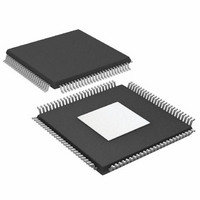
IC,D/A CONVERTER,DUAL,16-BIT,CMOS,TQFP,100PIN
Manufacturer
Analog Devices Inc
Series
TxDAC®r
Datasheet
1.AD9785BSVZ.pdf
(64 pages)
Specifications of AD9788BSVZRL
Design Resources
Powering the AD9788 Using ADP2105 for Increased Efficiency (CN0141)
Number Of Bits
16
Data Interface
Serial
Number Of Converters
2
Voltage Supply Source
Analog and Digital
Power Dissipation (max)
450mW
Operating Temperature
-40°C ~ 85°C
Mounting Type
Surface Mount
Package / Case
100-TQFP Exposed Pad, 100-eTQFP, 100-HTQFP, 100-VQFP
Lead Free Status / RoHS Status
Lead free / RoHS Compliant
For Use With
AD9788-EBZ - BOARD EVAL FOR AD9788
Settling Time
-
Lead Free Status / RoHS Status
Lead free / RoHS Compliant
Available stocks
Company
Part Number
Manufacturer
Quantity
Price
Company:

Part Number:
AD9788BSVZRL
Manufacturer:
Analog Devices Inc
Quantity:
10 000
Part Number:
AD9788BSVZRL
Manufacturer:
ADI/亚德诺
Quantity:
20 000


SPECIFICATIONS
DC SPECIFICATIONS
T
otherwise noted. LVDS driver and receiver are compliant to the IEEE 1596 reduced range link, unless otherwise noted.
Table 1.
Parameter
RESOLUTION
ACCURACY
MAIN DAC OUTPUTS
MAIN DAC TEMPERATURE DRIFT
AUX DAC OUTPUTS
REFERENCE
ANALOG SUPPLY VOLTAGES
DIGITAL SUPPLY VOLTAGES
POWER CONSUMPTION
OPERATING RANGE
1
Based on a 10 Ω external resistor.
MIN
Differential Nonlinearity (DNL)
Integral Nonlinearity (INL)
Offset Error
Gain Error (with Internal Reference)
Full-Scale Output Current
Output Compliance Range
Output Resistance
Gain DAC Monotonicity
Settling Time, to Within ±0.5 LSBs
Offset
Gain
Reference Voltage
Resolution
Full-Scale Output Current
Output Compliance Range (Source)
Output Compliance Range (Sink)
Output Resistance
Aux DAC Monotonicity Guaranteed
Internal Reference Voltage
Output Resistance
AVDD33
CVDD18
DVDD33
DVDD18
1× Mode, f
2× Mode, f
4× Mode, f
8× Mode, f
Power-Down Mode
to T
Guaranteed
PLL Off, IF = 2 MHz
Inverse Sinc Off, PLL Off
Inverse Sinc Off, PLL Off
Inverse Sinc Off, PLL Off
MAX
, AVDD33 = 3.3 V, DVDD33 = 3.3 V, DVDD18 = 1.8 V, CVDD18 = 1.8 V, I
DATA
DATA
DATA
DATA
= 100 MSPS,
= 100 MSPS,
= 100 MSPS,
= 100 MSPS,
1
Min
–0.001
8.66
–1.0
–1.998
0
0.8
3.13
1.70
3.13
1.70
–40
AD9785
Typ
12
±0.2
±0.3
0
±2
20.2
10
10
20
0.04
100
30
10
1
10
1.2
5
3.3
1.8
3.3
1.8
375
533
754
1054
2.5
+25
Max
+0.001
31.66
+1.0
+1.998
1.6
1.6
3.47
1.90
3.47
1.90
450
9.0
+85
Rev. A | Page 3 of 64
Min
−0.001
8.66
–1.0
–1.998
0
0.8
3.13
1.70
3.13
1.70
–40
AD9787
Typ
14
±0.5
±1.0
0
±2
20.2
10
10
20
0.04
100
30
10
1
10
1.2
5
3.3
1.8
3.3
1.8
375
533
754
1054
2.5
+25
OUTFS
Max
+0.001
31.66
+1.0
+1.998
1.6
1.6
3.47
1.90
3.47
1.90
450
9.0
+85
= 20 mA, maximum sample rate, unless
AD9785/AD9787/AD9788
Min
−0.001
8.66
–1.0
–1.998
0
0.8
3.13
1.70
3.13
1.70
–40
AD9788
Typ
16
±2.1
±3.7
0
±2
20.2
10
10
20
0.04
100
30
10
1
10
1.2
5
3.3
1.8
3.3
1.8
375
533
754
1054
2.5
+25
Max
+0.001
31.66
+1.998
1.6
1.6
3.47
1.90
450
9.0
+85
+1.0
3.47
1.90
Unit
Bits
LSB
LSB
% FSR
% FSR
mA
V
MΩ
Bits
ns
ppm/°C
ppm/°C
ppm/°C
Bits
mA
V
V
MΩ
Bits
V
kΩ
V
V
V
V
mW
mW
mW
mW
mW
°C
Related parts for AD9788BSVZRL
Image
Part Number
Description
Manufacturer
Datasheet
Request
R

Part Number:
Description:
±1.7g Dual-Axis IMEMS Accelerometer Evaluation Board
Manufacturer:
Analog Devices Inc
Datasheet:

Part Number:
Description:
Inertial Sensor Evaluation System
Manufacturer:
Analog Devices Inc
Datasheet:
Part Number:
Description:
Manufacturer:
Analog Devices Inc
Datasheet:
Part Number:
Description:
Manufacturer:
Analog Devices Inc
Datasheet:
Part Number:
Description:
Manufacturer:
Analog Devices Inc
Datasheet:
Part Number:
Description:
Manufacturer:
Analog Devices Inc
Datasheet:
Part Number:
Description:
Manufacturer:
Analog Devices Inc
Datasheet:
Part Number:
Description:
Manufacturer:
Analog Devices Inc
Datasheet:
Part Number:
Description:
Manufacturer:
Analog Devices Inc
Datasheet:
Part Number:
Description:
Manufacturer:
Analog Devices Inc
Datasheet:
Part Number:
Description:
Manufacturer:
Analog Devices Inc
Datasheet:
Part Number:
Description:
Manufacturer:
Analog Devices Inc
Datasheet:
Part Number:
Description:
Manufacturer:
Analog Devices Inc
Datasheet: