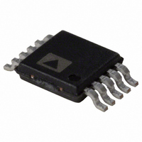
AD9833BRM Analog Devices Inc, AD9833BRM Datasheet - Page 15

AD9833BRM
Manufacturer Part Number
AD9833BRM
Description
10 Bit, 10 Pin DDS
Manufacturer
Analog Devices Inc
Datasheet
1.AD9833BRMZ.pdf
(24 pages)
Specifications of AD9833BRM
Rohs Status
RoHS non-compliant
Resolution (bits)
10 b
Master Fclk
25MHz
Tuning Word Width (bits)
28 b
Voltage - Supply
2.3 V ~ 5.5 V
Operating Temperature
-40°C ~ 105°C
Mounting Type
Surface Mount
Package / Case
10-MSOP, Micro10™, 10-uMAX, 10-uSOP
Resolution
10 Bit
Maximum Input Frequency
25 MHz
Tuning Word Width
28 Bit
Minimum Operating Supply Voltage
2.3 V
Typical Operating Supply Voltage
2.5|3.3|5 V
Maximum Operating Supply Voltage
5.5 V
Minimum Operating Temperature
-40 °C
Maximum Operating Temperature
105 °C
Lead Free Status / RoHS Status
Contains lead / RoHS non-compliant
For Use With
EVAL-AD9833EBZ - BOARD EVAL FOR AD9833
Lead Free Status / RoHS Status
Contains lead / RoHS non-compliant
Available stocks
Company
Part Number
Manufacturer
Quantity
Price
Part Number:
AD9833BRM
Manufacturer:
ADI/亚德诺
Quantity:
20 000
Company:
Part Number:
AD9833BRMZ
Manufacturer:
MICRON
Quantity:
2 154
Company:
Part Number:
AD9833BRMZ
Manufacturer:
ADI
Quantity:
5 000
Part Number:
AD9833BRMZ
Manufacturer:
ADI/亚德诺
Quantity:
20 000
Part Number:
AD9833BRMZ-REEL
Manufacturer:
ADI/亚德诺
Quantity:
20 000
Company:
Part Number:
AD9833BRMZ-REEL7
Manufacturer:
AD
Quantity:
14 592
Part Number:
AD9833BRMZ-REEL7
Manufacturer:
ADI/亚德诺
Quantity:
20 000
FREQUENCY AND PHASE REGISTERS
The AD9833 contains two frequency registers and two phase
registers, which are described in Table 7.
Table 7. Frequency/Phase Registers
Register
FREQ0
FREQ1
PHASE0
PHASE1
The analog output from the AD9833 is
where FREQREG is the value loaded into the selected frequency
register. This signal will be phase shifted by
where PHASEREG is the value contained in the selected phase
register. Consideration must be given to the relationship of the
selected output frequency and the reference clock frequency to
avoid unwanted output anomalies.
The flowchart in Figure 28 shows the routine for writing to the
frequency and phase registers of the AD9833.
Writing to a Frequency Register
When writing to a frequency register, Bit D15 and Bit D14 give
the address of the frequency register.
Table 8. Frequency Register Bits
D15
0
1
If the user wants to change the entire contents of a frequency
register, two consecutive writes to the same address must be
performed because the frequency registers are 28 bits wide. The
first write contains the 14 LSBs, and the second write contains
the 14 MSBs. For this mode of operation, the B28 (D13) control
bit should be set to 1. An example of a 28-bit write is shown in
Table 9.
f
2 π/4096 × PHASEREG
MCLK
/2
D14
1
0
28
Size
28 bits
28 bits
12 bits
12 bits
× FREQREG
D13
MSB 14 FREQ0 REG bits
MSB 14 FREQ1 REG bits
Description
Frequency Register 0. When the FSELECT
bit = 0, this register defines the output
frequency as a fraction of the MCLK
frequency.
Frequency Register 1. When the FSELECT
bit = 1, this register defines the output
frequency as a fraction of the MCLK
frequency.
Phase Offset Register 0. When the PSELECT
bit = 0, the contents of this register are
added to the output of the phase
accumulator.
Phase Offset Register 1. When the PSELECT
bit = 1, the contents of this register are
added to the output of the phase
accumulator.
D0
LSB
LSB
Rev. C | Page 15 of 24
Table 9. Writing 00FC00 to FREQ0 REG
SDATA Input
0010 0000 0000 0000
0100 0000 0000 0000
0100 0000 0011 1111
In some applications, the user does not need to alter all 28 bits
of the frequency register. With coarse tuning, only the 14 MSBs
are altered, while with fine tuning, only the 14 LSBs are altered.
By setting the B28 (D13) control bit to 0, the 28-bit frequency
register operates as two, 14-bit registers, one containing the 14 MSBs
and the other containing the 14 LSBs. This means that the 14 MSBs
of the frequency word can be altered independent of the 14 LSBs,
and vice versa. Bit HLB (D12) in the control register identifies
which 14 bits are being altered. Examples of this are shown in
Table 10 and Table 11.
Table 10. Writing 3FFF to the 14 LSBs of FREQ1 REG
SDATA Input
0000 0000 0000 0000
1011 1111 1111 1111
Table 11. Writing 00FF to the 14 MSBs of FREQ0 REG
SDATA Input
0001 0000 0000 0000
0100 0000 1111 1111
Writing to a Phase Register
When writing to a phase register, Bit D15 and Bit D14 are set to 11.
Bit D13 identifies which phase register is being loaded.
Table 12. Phase Register Bits
D15
1
1
D14
1
1
D13
0
1
Result of Input Word
Control word write (D15, D14 = 00),
B28 (D13) = 0; HLB (D12) = 0, that is, LSBs
FREQ1 REG write (D15, D14 = 10),
14 LSBs = 3FFF
Result of Input Word
Control word write (D15, D14 = 00),
B28 (D13) = 0, HLB (D12) = 1, that is, MSBs
FREQ0 REG write (D15, D14 = 01),
14 MSBs = 00FF
D12
X
X
Result of Input Word
Control word write (D15, D14 = 00),
B28 (D13) = 1, HLB (D12) = X
FREQ0 REG write (D15, D14 = 01),
14 LSBs = 0000
FREQ0 REG write (D15, D14 = 01),
14 MSBs = 003F
D11
MSB 12 PHASE0 bits
MSB 12 PHASE1 bits
AD9833
D0
LSB
LSB


