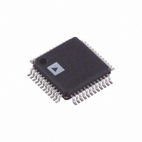
AD9940BSTZ Analog Devices Inc, AD9940BSTZ Datasheet

AD9940BSTZ
Specifications of AD9940BSTZ
Available stocks
Related parts for AD9940BSTZ
AD9940BSTZ Summary of contents
Page 1
FEATURES 56 MSPS correlated double sampler (CDS) with 6 dB gain On-chip horizontal and RG timing driver Single-supply operation (2.7 V min ) Precision Timing™ core with 0.37 ns resolution at 56 MSPS Low power CMOS: 105 mW at 2.7 ...
Page 2
AD9940 TABLE OF CONTENTS Specifications..................................................................................... 3 Analog Specifications................................................................... 4 Digital Specifications ................................................................... 5 Timing Specifications (Slave Timing Mode) ............................ 5 Absolute Maximum Ratings............................................................ 6 Thermal Characteristics .............................................................. 6 ESD Caution.................................................................................. 6 Pin Configuration and Function Descriptions............................. 7 Data Bit Descriptions ...
Page 3
SPECIFICATIONS Table 1. Parameter TEMPERATURE RANGE Operating Storage MAXIMUM CLOCK RATE POWER SUPPLY VOLTAGE AVDD, TCVDD (AFE, Timing Core) OVDD (Analog Buffer) DVDD (Digital) HVDD ( Drivers) RGVDD (RG Driver) 1 POWER DISSIPATION 56 MHz, AFE supplies = ...
Page 4
AD9940 ANALOG SPECIFICATIONS MHz, AVDD = OVDD = DVDD = TCVDD = 3.0 V, −25°C to +85°C, unless otherwise noted. CLI Table 2. Parameter CDS Gain 1 Allowable CCD Reset Transient Maximum Input Range Before Saturation 1 ...
Page 5
DIGITAL SPECIFICATIONS AVDD = DVDD = OVDD = TCVDD = HVDD = RGVDD = 2.7 V, −25°C to +85°C, unless otherwise noted. MIN MAX Table 3. Parameter LOGIC INPUTS High Level Input Voltage Low Level Input ...
Page 6
AD9940 ABSOLUTE MAXIMUM RATINGS Table 5. Parameter AVDD and TCVDD to AVSS HVDD and RGVDD to HVSS and RGVSS DVDD and OVDD to DVSS and OVSS Any VSS to Any VSS CLPOB/HBLK to DVSS SCK, SL, and SDI to DVSS ...
Page 7
PIN CONFIGURATION AND FUNCTION DESCRIPTIONS Table 6. Pin Function Descriptions 1 Pin No. Menumonic Type AVSS P 3 AVDD P 4 DIFFN AO 5 DIFFP AO 6 OVSS P 7 OVDD P 8 TCVDD P 9 ...
Page 8
AD9940 1 Pin No. Menumonic Type 33 SHP DI 34 AVSS P 35 CCDIN AI 36 AVSS P 37 AVDD P 38 AVSS P 39 REFB AO 40 REFT 47, 48 AVSS P 1 ...
Page 9
DATA BIT DESCRIPTIONS Table 7. Address Data Bit Content Default Value 0 [0] 0 [1] 0 [2] 0 [3] 0 [4] 0 [6: [6: [0] 0 [1] 0 [2] 0 [3] 0 ...
Page 10
AD9940 Address Data Bit Content Default Value 7 [0] 0 [1] 0 [2] 0 [3] 0 [4] 0 [5] 0 [ [0] 0 [1] 0 [2] 0 [3] 0 [7: [0] 0 [1] 0 ...
Page 11
Address Data Bit Content Default Value 14 [2:0] 3 [3] 0 [6: [5:0] 0 [7:6] — 16 [5:0] 24 [7: [5:0] 0 [7:6] — 18 [5:0] 24 [7:6] — 19 [3:0] 7 [7:4] 7 ...
Page 12
AD9940 SERIAL INTERFACE TIMING All the internal registers of the AD9940 are accessed through a 3-wire serial interface. Each register consists of an 8-bit data byte starting with the LSB bit. As shown in bits are clocked in on the ...
Page 13
SYSTEM OVERVIEW Figure 6 shows the typical system block diagram for the AD9940. The CCD output is processed by the AD9940’s AFE circuitry, which consists of a correlated double sam- pler (CDS) and output buffer. The differential output of the ...
Page 14
AD9940 PRECISION TIMING, HIGH SPEED TIMING GENERATION The AD9940 generates flexible, high speed timing signals using the Precision Timing core. This core is the foundation for generating the timing used for both the CCD and the AFE: the reset gate ...
Page 15
CCD SIGNAL H1/ H2/ PROGRAMMABLE CLOCK POSITIONS POLARITY RISING EDGE FALLING EDGE. 4 SHP SAMPLE LOCATION. 5 SHD SAMPLE LOCATION. 6 H1/H3 ...
Page 16
AD9940 H-DRIVER AND RG OUTPUTS In addition to the programmable timing positions, the AD9940 features on-chip output drivers for the RG and out- puts. These drivers are powerful enough to directly drive the CCD inputs. The H-driver ...
Page 17
HBLK SEQUENCES The HBLK programmable timing shown in Figure 12 is programmed using the HBLKTOG registers. Only the toggle positions are used to designate the start and the stop posi- tions of the blanking period. Additionally, a polarity control, HBLKMASKPOL, ...
Page 18
AD9940 HD 1 HBLK H1/H3 H2/H4 SPECIAL H-BLANK PATTERN IS CREATED USING MULTIPLE HBLK TOGGLE POSITIONS. PROGRAMMABLE SETTINGS: 1 HBLKTOG1_0 2 HBLKTOG2_0 3 HBLKTOG1_1 4 HBLKTOG2_1 5 HBLKTOG1_2 6 HBLKTOG2_2 Figure 14. Generating Special HBLK Patterns ...
Page 19
APPLICATIONS INFORMATION All signals should be carefully routed on the PCB to main- tain low noise performance. The CCD output signal should be connected to the CCDIN pin through a 0.1 μF capacitor. The CCD timing signals H1A/B to H2A/B ...
Page 20
... SEATING PLANE ORDERING GUIDE Model Temperature Range 1 AD9940BSTZ −25°C to +85°C 1 AD9940BSTZRL −25°C to +85°C 1 AD9940BCPZ −25°C to +85°C 1 AD9940BCPZRL −25°C to +85° Pb-free part. ©2005 Analog Devices, Inc. All rights reserved. Trademarks and registered trademarks are the property of their respective owners. ...


