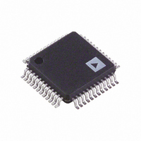
AD9952YSVZ-REEL7 Analog Devices Inc, AD9952YSVZ-REEL7 Datasheet - Page 16

AD9952YSVZ-REEL7
Manufacturer Part Number
AD9952YSVZ-REEL7
Description
IC,FREQUENCY SYNTHESIZER,CMOS,TQFP,48PIN,PLASTIC
Manufacturer
Analog Devices Inc
Datasheet
1.AD9952YSVZ.pdf
(28 pages)
Specifications of AD9952YSVZ-REEL7
Resolution (bits)
14 b
Master Fclk
400MHz
Tuning Word Width (bits)
32 b
Voltage - Supply
1.71 V ~ 1.96 V
Operating Temperature
-40°C ~ 105°C
Mounting Type
Surface Mount
Package / Case
48-TQFP Exposed Pad, 48-eTQFP, 48-HTQFP, 48-VQFP
Lead Free Status / RoHS Status
Lead free / RoHS Compliant
For Use With
AD9952/PCB - BOARD EVAL FOR AD9952
Lead Free Status / Rohs Status
Compliant
Available stocks
Company
Part Number
Manufacturer
Quantity
Price
Company:
Part Number:
AD9952YSVZ-REEL7
Manufacturer:
Analog Devices Inc
Quantity:
10 000
AD9952
CONTROL REGISTER BIT DESCRIPTIONS
Control Function Register 1 (CFR1)
The CFR1 bits control the functions, features, and modes of the
AD9952. The functionality of each bit is detailed below.
CFR1 [31:27]: Not Used
CFR1 [26]: Amplitude Ramp Rate Load Control Bit
CFR1 [26] = 0 (default). The amplitude ramp rate timer is
loaded only upon timeout (timer = 1) and is not loaded due to
an I/O UPDATE input signal.
CFR1 [26] = 1. The amplitude ramp rate timer is loaded upon
timeout (timer = 1) or at the time of an I/O UPDATE input
signal.
CFR1 [25]: Shaped On-Off Keying Enable Bit
CFR1 [25] = 0 (default). Shaped on-off keying is bypassed.
CFR1 [25] = 1. Shaped on-off keying is enabled. When enabled,
CFR1 [24] controls the mode of operation for this function.
CFR1 [24]: Auto Shaped On-Off Keying Enable Bit (only
valid when CFR1[25] is active high)
CFR1 [24] = 0 (default). When CFR1[25] is active, a Logic 0 on
CFR1[24] enables the manual shaped on-off keying operation.
Each amplitude sample sent to the DAC is multiplied by the
amplitude scale factor. See the Shaped On-Off Keying section
for details.
CFR1 [24] = 1. When CFR1[25] is active, a Logic 1 on CFR1
[24] enables the auto shaped on-off keying operation. Toggling
the OSK pin high causes the output scalar to ramp up from zero
scale to the amplitude scale factor at a rate determined by the
amplitude ramp rate. Toggling the OSK pin low causes the
output to ramp down from the amplitude scale factor to zero
scale at the amplitude ramp rate (see the Shaped On-Off Keying
section).
CFR1 [23]: Automatic Synchronization Enable Bit
CFR1 [23] = 0 (default). The automatic synchronization feature
of multiple AD9952s is inactive.
CFR1 [23] = 1. The automatic synchronization feature of
multiple AD9952s is active. The device synchronizes its internal
synchronization clock (SYNC_CLK) to align to the signal
present on the SYNC_IN input (see the Synchronizing Multiple
AD9952 section).
CFR1 [22]: Software Manual Synchronization of Multiple
AD9952s
CFR1 [22] = 0 (default). The manual synchronization feature is
inactive.
Rev. B | Page 16 of 28
CFR1 [22] = 1. The software controlled manual synchronization
feature is executed. The SYNC_CLK rising edge is advanced by
one SYNC_CLK cycle and this bit is cleared. To advance the
rising edge multiple times, this bit needs to be set for each
advance (see the Synchronizing Multiple AD9952 section).
CFR1 [21:14]: Not Used
CFR1 [13]: Auto-Clear Phase Accumulator Bit
CFR1 [13] = 0 (default). The current state of the phase
accumulator remains unchanged when the frequency tuning
word is applied.
CFR1 [13] = 1. This bit synchronously clears the phase
accumulator automatically (by loadings 0s) for one cycle upon
reception of an I/O UPDATE signal.
CFR1 [12]: Sine/Cosine Select Bit
CFR1 [12] = 0 (default). The angle-to-amplitude conversion
logic employs a COSINE function.
CFR1 [12] = 1. The angle-to-amplitude conversion logic
employs a SINE function.
CFR1 [11]: Not Used
CFR1 [10]: Clear Phase Accumulator
CFR1 [10] = 0 (default). The phase accumulator functions as
normal.
CFR1 [10] = 1. The phase accumulator memory elements are
cleared and held clear until this bit is cleared.
CFR1 [9]: SDIO Input Only
CFR1 [9] = 0 (default). The SDIO pin has bidirectional
operation (2-wire serial programming mode).
CFR1 [9] = 1. The serial data I/O pin (SDIO) is configured as
an input only pin (3-wire serial programming mode).
CFR1 [8]: LSB First
CFR1 [8] = 0 (default). MSB first format is active.
CFR1 [8] = 1. The serial interface accepts serial data in LSB-first
format.
CFR1 [7]: Digital Power-Down Bit
CFR1 [7] = 0 (default). All digital functions and clocks are active.
CFR1 [7] = 1. All non-I/O digital functionality is suspended,
lowering the power significantly.


