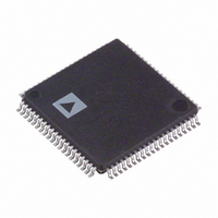
AD9985KSTZ-140 Analog Devices Inc, AD9985KSTZ-140 Datasheet - Page 24

AD9985KSTZ-140
Manufacturer Part Number
AD9985KSTZ-140
Description
IC,Data Acquisition Signal Conditioner,3-CHANNEL,8-BIT,CMOS,QFP,80PIN,PLASTIC
Manufacturer
Analog Devices Inc
Datasheet
1.AD9985KSTZ-110.pdf
(32 pages)
Specifications of AD9985KSTZ-140
Applications
Video
Interface
Serial Port
Voltage - Supply
2.2 V ~ 3.45 V
Package / Case
80-LQFP
Mounting Type
Surface Mount
Lead Free Status / RoHS Status
Lead free / RoHS Compliant
Available stocks
Company
Part Number
Manufacturer
Quantity
Price
Company:
Part Number:
AD9985KSTZ-140
Manufacturer:
ADI
Quantity:
717
Company:
Part Number:
AD9985KSTZ-140
Manufacturer:
Analog Devices Inc
Quantity:
10 000
Part Number:
AD9985KSTZ-140
Manufacturer:
ADI/亚德诺
Quantity:
20 000
AD9985
Table 33. Detected Hsync Input Polarity Status
Hsync Polarity
Status
0
1
14
Table 34. Vsync Detection Results
Detect
0
1
14
Table 35. Active Vsync Results
Bit 4, Reg 14H
(Vsync Detect)
1
0
X
14
Table 36. Detected Vsync Output Polarity Status
Vsync Polarity Status
0
1
14
4
This bit is used to indicate when activity is detected on
the Vsync input pin (Pin 31). If Vsync is held steady
high or low, activity will not be detected.
The Sync Processing Block Diagram (Figure 14) shows
where this function is implemented.
3
This bit indicates which Vsync source is being used:
the Vsync input or output from the sync separator.
Bit 4 in this register determines which is active. If both
Vsync and SOG are detected, the user can determine
which has priority via Bit 0 in Register 0EH. The user
can override this function via Bit 1 in Register 0EH. If
the override bit is set to Logic 1, this bit will be forced
to whatever the state of Bit 0 in Register 0EH is set to.
AVS = 0 means Vsync input.
AVS = 1 means Sync separator.
The override bit is in Register 0EH, Bit 1.
2
This bit reports the status of the Vsync output polarity
detection circuit. It can be used to determine the
polarity of the Vsync output. The detection circuit’s
location is shown in the Sync Processing Block
Diagram (Figure 14).
1
This bit is used to indicate when sync activity is
detected on the Sync-on-Green input pin (Pin 49).
Vsync Detect
AVS – Active Vsync
Detected Vsync Output Polarity Status
Sync-on-Green Detect
Function
No Activity Detected
Activity Detected
Result
Negative
Positive
Bit 1, Reg 0EH
(Override)
0
0
1
Result
Active Low
Active High
AVS
0
1
Bit 0 in 0EH
Rev. 0 | Page 24 of 32
Table 37. Sync-on-Green Detection Results
Detect
0
1
14
Table 38. Detected Coast Input Polarity Status
Polarity Status
0
1
15
Table 39. 4:2:2 Output Mode Select
Select
0
1
Table 40. 4:2:2 Input/Output Configuration
Channel
Red
Green
Blue
19
1A
The Sync Processing Block Diagram (Figure 14) shows
where this function is implemented.
0
This bit reports the status of the Coast input polarity
detection circuit. It can be used to determine the
polarity of the Coast input. The detection circuit’s
location is shown in the Sync Processing Block
Diagram (Figure 14).
This indicates that Bit 1 of Register 5 is the 4:2:2
output mode select bit.
1
This bit configures the output data in 4:2:2 mode. This
mode can be used to reduce the number of data lines
used from 24 down to 16 for applications using YUV,
YCbCr, or YPbPr graphics signals. A timing diagram
for this mode is shown in Figure 11.
Recommended input and output configurations are
shown in Table 39.
7:0
This specifies the targeted value of the final offset for
the Red channel when auto offset is employed
(Register 0x1D Bit 7 = 1). Default is 4.
7:0
This specifies the targeted value of the final offset for
the Green channel when auto offset is employed
(Register 0x1D Bit 7 = 1). Default is 4.
Detected Coast Polarity Status
4:2:2 Output Mode Select
Input
Connection
V
Y
U
Red Target Code
Green Target Code
Function
No Activity Detected
Activity Detected
Result
Coast Polarity Negative
Coast Polarity Positive
Output Mode
4:2:2
4:4:4
Output Format
U/V
Y
High Impedance


