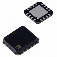
ADA4304-2ACPZ-R7 Analog Devices Inc, ADA4304-2ACPZ-R7 Datasheet

ADA4304-2ACPZ-R7
Specifications of ADA4304-2ACPZ-R7
Available stocks
Related parts for ADA4304-2ACPZ-R7
ADA4304-2ACPZ-R7 Summary of contents
Page 1
... CATV distribution systems Splitter modules Digital cable ready (DCR) TVs GENERAL DESCRIPTION The ADA4304 Ω active splitter for use in applications where a lossless signal split is required. Typical applications include multituner digital set-top boxes, cable splitter modules, multituner/digital cable ready (DCR) televisions, and home gateways where traditional solutions require discrete passive splitter modules with separate fixed gain amplifiers ...
Page 2
... ADA4304-2 TABLE OF CONTENTS Features .............................................................................................. 1 Applications....................................................................................... 1 Functional Block Diagram .............................................................. 1 General Description ......................................................................... 1 Revision History ............................................................................... 2 Specifications..................................................................................... 3 Absolute Maximum Ratings............................................................ 4 Thermal Resistance ...................................................................... 4 ESD Caution.................................................................................. 4 Pin Configuration and Function Descriptions............................. 5 REVISION HISTORY 5/07—Revision 0: Initial Version Typical Performance Characteristics ..............................................6 Test Circuits........................................................................................8 Applications........................................................................................9 Circuit Description .......................................................................9 Evaluation Boards .........................................................................9 RF Layout Considerations ...
Page 3
... See Figure 17, Figure 18, and Figure 19 Either output, 54 MHz to 865 MHz @ 54 MHz @ 550 MHz @ 865 MHz Either output, 54 MHz to 865 MHz @ 54 MHz @ 550 MHz @ 865 MHz Output referred 100 MHz Rev Page ADA4304-2 Min Typ Max Unit 1600 MHz 54 865 MHz 2.8 ...
Page 4
... The power dissipated in the package (P the quiescent power dissipation; the supply voltage (V Rating the quiescent current (I 5.5 V dissipation of the ADA4304-2 can be calculated as See Figure (MAX) −65°C to +125°C Airflow increases heat dissipation, effectively reducing θ −40°C to +85°C In addition, more metal directly in contact with the package 300° ...
Page 5
... PIN 1 INDICATOR 12 VOUT1 VCC 1 ADA4304-2 VCC 2 11 GND TOP VIEW GND 3 10 VOUT2 (Not to Scale) VIN 4 9 GND CONNECT Figure 4. Pin Configuration Mnemonic VCC GND VIN NC VOUT2 VOUT1 IL Rev Page ADA4304-2 Description Supply Pin Ground Input No Connection Output 2 Output 1 Bias Pin ...
Page 6
... ADA4304-2 TYPICAL PERFORMANCE CHARACTERISTICS Ω system 25°C, unless otherwise noted –54 –56 –58 – +85°C A –62 –64 – –40°C A –68 –70 –72 –74 50 100 FREQUENCY (MHz) Figure 5. Composite Second Order (CSO) vs. Frequency – 60 – 63 – 66 – 69 – +85°C A – 75 – – ...
Page 7
... Figure 15. Output Return Loss ( –60 –50 –40 –30 –20 – 100 4000 Figure 16. Quiescent Supply Current vs. Temperature ) vs. Frequency Rev Page ADA4304-2 100 FREQUENCY (MHz) Figure 14. Input Return Loss (S ) vs. Frequency 11 100 FREQUENCY (MHz vs. Frequency 22 33 TEMPERATURE (°C) 1000 1000 ...
Page 8
... ADA4304-2 TEST CIRCUITS RF NETWORK ANALYZER 75Ω S-PARAMETER TEST SET VOUT1 PORT 2 12 VIN DUT 4 PORT 1 10 VOUT2 PORT 3 75Ω Figure 17. Test Circuit for Measurements NETWORK ANALYZER 75Ω S-PARAMETER TEST SET VOUT1 PORT 2 12 VIN DUT 4 PORT 1 10 VOUT2 PORT 3 Figure 18. Test Circuit for S ...
Page 9
... The ADA4304-2 exhibits composite second order (CSO) and composite triple beat (CTB) products that are −62 dBc and −72 dBc, respectively. The use of the SiGe bipolar process also allows the ADA4304-2 to achieve a noise figure (NF dB. CIRCUIT DESCRIPTION The ADA4304-2 consists of a low noise buffer amplifier followed by a resistive power divider ...
Page 10
... ADA4304-2 Figure 21. ADA4304-2 Evaluation Board Figure 22. Evaluation Board Component Layout Rev Page ...
Page 11
... OUTLINE DIMENSIONS PIN 1 INDICATOR 1.00 0.85 0.80 SEATING PLANE ORDERING GUIDE Model Temperature Range 1 ADA4304-2ACPZ-RL −40°C to +85°C 1 ADA4304-2ACPZ-R7 −40°C to +85°C 1 ADA4304-2ACPZ-R2 −40°C to +85° RoHS Compliant Part. 3.00 0.60 MAX BSC SQ 0.45 TOP 2.75 VIEW BSC SQ ...
Page 12
... ADA4304-2 NOTES ©2007 Analog Devices, Inc. All rights reserved. Trademarks and registered trademarks are the property of their respective owners. D06539-0-5/07(0) Rev Page ...


