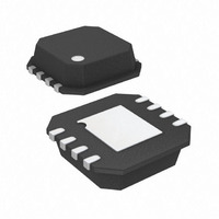
ADA4817-1ACPZ-RL Analog Devices Inc, ADA4817-1ACPZ-RL Datasheet - Page 17

ADA4817-1ACPZ-RL
Manufacturer Part Number
ADA4817-1ACPZ-RL
Description
Hi Speed FET Input Amp
Manufacturer
Analog Devices Inc
Series
FastFET™r
Datasheet
1.ADA4817-1ACPZ-R7.pdf
(24 pages)
Specifications of ADA4817-1ACPZ-RL
Amplifier Type
Voltage Feedback
Number Of Circuits
1
Slew Rate
870 V/µs
Gain Bandwidth Product
410MHz
-3db Bandwidth
1.05GHz
Current - Input Bias
2pA
Voltage - Input Offset
400µV
Current - Supply
19mA
Current - Output / Channel
40mA
Voltage - Supply, Single/dual (±)
5 V ~ 10 V, ±2.5 V ~ 5 V
Operating Temperature
-40°C ~ 105°C
Mounting Type
Surface Mount
Package / Case
8-LFCSP
Lead Free Status / RoHS Status
Lead free / RoHS Compliant
Output Type
-
Lead Free Status / RoHS Status
Lead free / RoHS Compliant
LEAKAGE CURRENTS
Poor PCB layout, contaminants, and the board insulator
material can create leakage currents that are much larger than
the input bias current of the ADA4817-1/ADA4817-2. Any
voltage differential between the inputs and nearby runs sets
up leakage currents through the PCB insulator, for example, 1 V/
100 GΩ = 10 pA. Similarly, any contaminants, such as skin oils
on the board, can create significant leakage. To reduce leakage
significantly, put a guard ring (shield) around the inputs and
input leads that are driven to the same voltage potential as the
inputs. This way there is no voltage potential between the inputs
and surrounding area to set up any leakage currents. For the
guard ring to be completely effective, it must be driven by a
relatively low impedance source and should completely
surround the input leads on all sides (above and below)
while using a multilayer board.
Another effect that can cause leakage currents is the charge
absorption of the insulator material itself. Minimizing the amount
of material between the input leads and the guard ring helps to
reduce the absorption. In addition, low absorption materials,
such as Teflon® or ceramic, can be necessary in some instances.
Rev. 0 | Page 17 of 24
INPUT CAPACITANCE
Along with bypassing and ground, high speed amplifiers can be
sensitive to parasitic capacitance between the inputs and ground.
A few picofarads of capacitance reduces the input impedance at
high frequencies, in turn increasing the amplifier’s gain, causing
peaking of the frequency response or even oscillations if severe
enough. It is recommended that the external passive components
connected to the input pins be placed as close as possible to the
inputs to avoid parasitic capacitance. The ground and power
planes must be kept at a small distance from the input pins on
all layers of the board.
INPUT-TO-INPUT/OUTPUT COUPLING
To minimize capacitive coupling between the inputs and
outputs, the output signal traces should not be parallel with
the inputs. In addition, the input traces should not be very
close to each other. A minimum of 7 mils between the two
inputs is recommended.
ADA4817-1/ADA4817-2


