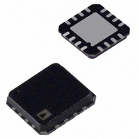
ADA4857-2YCPZ-R2 Analog Devices Inc, ADA4857-2YCPZ-R2 Datasheet - Page 16

ADA4857-2YCPZ-R2
Manufacturer Part Number
ADA4857-2YCPZ-R2
Description
IC,Operational Amplifier,DUAL,BIPOLAR,LLCC,16PIN,PLASTIC
Manufacturer
Analog Devices Inc
Datasheet
1.ADA4857-1YCPZ-R7.pdf
(20 pages)
Specifications of ADA4857-2YCPZ-R2
Amplifier Type
Voltage Feedback
Number Of Circuits
2
Slew Rate
2800 V/µs
-3db Bandwidth
850MHz
Current - Input Bias
2µA
Voltage - Input Offset
2000µV
Current - Supply
5mA
Current - Output / Channel
50mA
Voltage - Supply, Single/dual (±)
4.5 V ~ 10.5 V, ±2.25 V ~ 5.25 V
Operating Temperature
-40°C ~ 125°C
Mounting Type
Surface Mount
Package / Case
16-LFCSP
Lead Free Status / RoHS Status
Lead free / RoHS Compliant
Output Type
-
Gain Bandwidth Product
-
Lead Free Status / RoHS Status
Lead free / RoHS Compliant
ADA4857-1/ADA4857-2
APPLICATIONS INFORMATION
POWER-DOWN OPERATION
The PD pin is used to power down the chip, which reduces the
quiescent current and the overall power consumption. It is low
enabled, which means that the chip is on with full power when
the PD pin input voltage is low (see Table 8). Note that PD does not
put the output in a high-Z state, which means that the ADA4857
should not be used as a multiplexer.
Table 8. PD Operation Table Guide
Condition
Enabled
Powered down
Table 9. Various Gain and Recommended Resistor Values Associated with Conditions; V
Gain
+1
+2
+5
+10
R
0
499
499
499
F
(Ω)
R
N/A
499
124
56.2
G
(Ω)
±5 V
≤+0.8 V
≥+3 V
−3 dB SS BW (MHz),
V
850
360
90
43
OUT
= 200 mV p-p
Supply Voltage
±2.5 V
≤−1.7 V
≥+0.5 V
+5 V
≤+0.8 V
≥+3 V
Slew Rate (V/μs),
V
2350
1680
516
213
OUT
Rev. A | Page 16 of 20
= 2 V Step
CAPACITIVE LOAD CONSIDERATIONS
When driving a capacitive load using the SOIC package, R
used to reduce the peaking (see Figure 47). An optimum resistor
value of 40 Ω is found to maintain the peaking within 1 dB for
any capacitive load up to 40 pF.
RECOMMENDED VALUES FOR VARIOUS GAINS
Table 9 provides a useful reference for determining various gains
and associated performance. R
their contribution to the overall noise performance of the amplifier.
ADA4857 Voltage
Noise (nV/√Hz), RTO
4.4
8.8
22.11
43.47
S
= ±5 V, T
F
and R
A
= 25°C, R
G
are kept low to minimize
Total System
Noise (nV/√Hz), RTO
4.49
9.89
23.49
45.31
L
= 1 kΩ, R
T
= 49.9 Ω
SNUB
is


