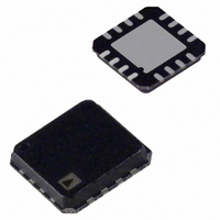
ADA4932-1YCPZ-RL Analog Devices Inc, ADA4932-1YCPZ-RL Datasheet - Page 8

ADA4932-1YCPZ-RL
Manufacturer Part Number
ADA4932-1YCPZ-RL
Description
Lw Cst/Lw Pwr Diff ADC Driver
Manufacturer
Analog Devices Inc
Datasheet
1.ADA4932-1YCPZ-R7.pdf
(28 pages)
Specifications of ADA4932-1YCPZ-RL
Design Resources
Single-Ended-to-Differential High Speed Drive Circuit for 16-Bit, 10 MSPS AD7626 ADC (CN0105)
Amplifier Type
Differential
Number Of Circuits
1
Output Type
Differential
Slew Rate
2800 V/µs
-3db Bandwidth
560MHz
Current - Input Bias
2.5µA
Voltage - Input Offset
500µV
Current - Supply
9.6mA
Current - Output / Channel
80mA
Voltage - Supply, Single/dual (±)
3 V ~ 11 V, ±1.5 V ~ 5.5 V
Operating Temperature
-40°C ~ 105°C
Mounting Type
Surface Mount
Package / Case
16-LFCSP
Lead Free Status / RoHS Status
Lead free / RoHS Compliant
Gain Bandwidth Product
-
Lead Free Status / RoHS Status
Lead free / RoHS Compliant
ADA4932-1/ADA4932-2
PIN CONFIGURATIONS AND FUNCTION DESCRIPTIONS
Table 9. ADA4932-1 Pin Function Descriptions
Pin No.
1
2
3
4
5 to 8
9
10
11
12
13 to 16
17 (EPAD)
Table 10. ADA4932-2 Pin Function Descriptions
Pin No.
1
2
3, 4
5
6
7
8
9, 10
11
12
13
14
15, 16
17
18
19
20
21, 22
23
24
25 (EPAD)
–FB
+FB
NOTES
1. SOLDER EXPOSED PADDLE ON BACK OF PACKAGE
+IN
–IN
TO GROUND PLANE OR TO A POWER PLANE.
Mnemonic
−FB
+IN
−IN
+FB
+V
V
+OUT
−OUT
PD
−V
Exposed Paddle (EPAD)
Mnemonic
−IN1
+FB1
+V
−FB2
+IN2
−IN2
+FB2
+V
V
+OUT2
−OUT2
PD2
−V
V
+OUT1
−OUT1
PD1
−V
−FB1
+IN1
Exposed Paddle (EPAD)
1
2
3
4
OCM
OCM2
OCM1
Figure 5. ADA4932-1 Pin Configuration
S
S
S1
S2
S2
S1
ADA4932-1
(Not to Scale)
TOP VIEW
PIN 1
INDICATOR
12 PD
11 –OUT
10 +OUT
9 V
OCM
Description
Negative Output for Feedback Component Connection.
Positive Input Summing Node.
Negative Input Summing Node.
Positive Output for Feedback Component Connection.
Positive Supply Voltage.
Output Common-Mode Voltage.
Positive Output for Load Connection.
Negative Output for Load Connection.
Power-Down Pin.
Negative Supply Voltage.
Solder the exposed paddle on the back of the package to a ground plane or to a power plane.
Description
Negative Input Summing Node 1.
Positive Output Feedback 1.
Positive Supply Voltage 1.
Negative Output Feedback 2.
Positive Input Summing Node 2.
Negative Input Summing Node 2.
Positive Output Feedback 2.
Positive Supply Voltage 2.
Output Common-Mode Voltage 2.
Positive Output 2.
Negative Output 2.
Power-Down Pin 2.
Negative Supply Voltage 2.
Output Common-Mode Voltage 1.
Positive Output 1.
Negative Output 1.
Power-Down Pin 1.
Negative Supply Voltage 1.
Negative Output Feedback 1.
Positive Input Summing Node 1.
Solder the exposed paddle on the back of the package to a ground plane or to a power plane.
Rev. A | Page 8 of 28
+FB1
NOTES
1. SOLDER EXPOSED PADDLE ON BACK OF PACKAGE
–FB2
+V
+V
–IN1
+IN2
TO GROUND PLANE OR TO A POWER PLANE.
S1
S1
1
2
3
4
5
6
Figure 6. ADA4932-2 Pin Configuration
ADA4932-2
(Not to Scale)
TOP VIEW
PIN 1
INDICATOR
18
17
16
15
14
13
+OUT1
V
–V
–V
PD2
–OUT2
OCM1
S2
S2


