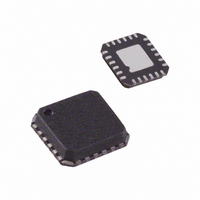
ADA4932-2YCPZ-R7 Analog Devices Inc, ADA4932-2YCPZ-R7 Datasheet - Page 22

ADA4932-2YCPZ-R7
Manufacturer Part Number
ADA4932-2YCPZ-R7
Description
Lw Cst/Lw Pwr Diff ADC Driver
Manufacturer
Analog Devices Inc
Datasheet
1.ADA4932-1YCPZ-R7.pdf
(28 pages)
Specifications of ADA4932-2YCPZ-R7
Amplifier Type
Differential
Number Of Circuits
2
Output Type
Differential
Slew Rate
2800 V/µs
-3db Bandwidth
560MHz
Current - Input Bias
2.5µA
Voltage - Input Offset
500µV
Current - Supply
9.6mA
Current - Output / Channel
80mA
Voltage - Supply, Single/dual (±)
3 V ~ 11 V, ±1.5 V ~ 5.5 V
Operating Temperature
-40°C ~ 105°C
Mounting Type
Surface Mount
Package / Case
24-LFCSP
Lead Free Status / RoHS Status
Lead free / RoHS Compliant
Gain Bandwidth Product
-
Lead Free Status / RoHS Status
Lead free / RoHS Compliant
Available stocks
Company
Part Number
Manufacturer
Quantity
Price
Company:
Part Number:
ADA4932-2YCPZ-R7
Manufacturer:
AD
Quantity:
1 670
ADA4932-1/ADA4932-2
input terminals due to negative voltage feedback and is in phase
with the input signal, thus reducing the effective voltage across
R
Terminating a Single-Ended Input
This section describes how to properly terminate a single-ended
input to the ADA4932-x with a gain of 1, R
499 Ω. An example using an input source with a terminated output
voltage of 1 V p-p and source resistance of 50 Ω illustrates the four
steps that must be followed. Note that because the terminated
output voltage of the source is 1 V p-p, the open-circuit output
voltage of the source is 2 V p-p. The source shown in Figure 59
indicates this open-circuit voltage.
1.
2.
2V p-p
G
in the upper loop and partially bootstrapping R
2V p-p
V
S
The input impedance is calculated using the formula
To match the 50 Ω source resistance, calculate the
termination resistor, R
closest standard 1% value for R
R
V
IN
S
Figure 59. Calculating Single-Ended Input Impedance, R
50Ω
,
R
se
S
50Ω
R
S
R
50Ω
1
IN, se
Figure 60. Adding Termination Resistor, R
R
665Ω
53.6Ω
IN, se
2
R
T
(
R
R
G
R
499Ω
499Ω
V
G
R
R
OCM
F
G
G
499Ω
V
499Ω
R
R
OCM
G
G
R
T
, using R
F
)
ADA4932-x
499Ω
499Ω
ADA4932-x
R
R
499Ω
499Ω
F
F
1
+V
–V
T
R
R
T
F
F
is 53.6 Ω.
+V
–V
S
S
||665 Ω = 50 Ω. The
2
S
S
(
F
499
= 499 Ω, and R
499
499
G
.
T
R
L
R
499
L
V
OUT, dm
IN
)
V
OUT, dm
G
Rev. A | Page 22 of 28
=
665
Ω
3.
1.03V p-p
Figure 60 shows that the effective R
loop is now greater than the R
addition of the termination resistors. To compensate for the
imbalance of the gain resistors, add a correction resistor (R
in series with R
equivalent of the source resistance, R
resistance, R
R
1 V p-p, which was obtained with R
circuit with the Thevenin equivalent (closest 1% value used for
R
loop is shown in Figure 62.
Figure 62 presents a tractable circuit with matched
feedback loops that can be easily evaluated.
It is useful to point out two effects that occur with a termi-
nated input. The first is that the value of R
both loops, lowering the overall closed-loop gain. The
second is that V
be if R
the output voltage, and for large resistor values in the feedback
loops (~1 kΩ), the effects essentially cancel each other out.
For small R
closed-loop gain is not canceled completely by the increased
V
The desired differential output in this example is 1 V p-p
because the terminated input signal was 1 V p-p and the
closed-loop gain = 1. The actual differential output voltage,
however, is equal to (1.03 V p-p)(499/524.5) = 0.98 V p-p.
To obtain the desired output voltage of 1 V p-p, a final gain
adjustment can be made by increasing R
any of the input circuitry. This is discussed in Step 4.
TS
TH
TH
Figure 62. Thevenin Equivalent and Matched Gain Resistors
V
) of the terminated source and R
= R
. This can be seen by evaluating Figure 62.
TH
2V p-p
T
TH
Figure 61. Calculating the Thevenin Equivalent
= 50 Ω. These two effects have opposite impacts on
V
25.5Ω
= R
25.5Ω
S
R
F
R
TH
and R
T
TS
, and is equal to R
S
||R
50Ω
R
G
S
TH
499Ω
499Ω
V
in the lower loop. R
T
R
R
OCM
G
= 25.9 Ω. Note that V
G
G
is a little larger than 1 V p-p, as it would
, or high gains, however, the diminished
R
53.6Ω
T
ADA4932-x
499Ω
499Ω
R
R
F
F
+V
–V
G
1.03V p-p
S
S
S
in the lower loop due to the
||R
TS
T
V
G
.
T
TH
TS
in the lower feedback
S
in the upper feedback
= 50 Ω. The modified
, and the termination
F
is the Thevenin
without modifying
G
TH
25.9Ω
R
is increased in
TH
is greater than
R
L
V
OUT, dm
TS
)


