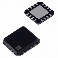
ADA4950-1YCPZ-R2 Analog Devices Inc, ADA4950-1YCPZ-R2 Datasheet - Page 14

ADA4950-1YCPZ-R2
Manufacturer Part Number
ADA4950-1YCPZ-R2
Description
Fixed Gain 1,2&3 Diff ADC Driver
Manufacturer
Analog Devices Inc
Type
Differential Amplifierr
Datasheet
1.ADA4950-1YCPZ-R7.pdf
(28 pages)
Specifications of ADA4950-1YCPZ-R2
Amplifier Type
Differential
Number Of Circuits
1
Output Type
Differential
Slew Rate
2900 V/µs
-3db Bandwidth
750MHz
Voltage - Input Offset
200µV
Current - Supply
9.5mA
Current - Output / Channel
114mA
Voltage - Supply, Single/dual (±)
3 V ~ 11 V, ±1.5 V ~ 5.5 V
Operating Temperature
-40°C ~ 105°C
Mounting Type
Surface Mount
Package / Case
16-LFCSP
No. Of Amplifiers
1
Input Offset Voltage
2.5mV
Bandwidth
750MHz
Supply Voltage Range
3V To 11V
Supply Current
9.5mA
Amplifier Case Style
LFCSP
No. Of Pins
16
Rohs Compliant
Yes
Number Of Channels
1
Number Of Elements
1
Power Supply Requirement
Single/Dual
Common Mode Rejection Ratio
49dB
Voltage Gain Db
66dB
Single Supply Voltage (typ)
5/9V
Dual Supply Voltage (typ)
±3/±5V
Power Supply Rejection Ratio
84dB
Rail/rail I/o Type
No
Single Supply Voltage (min)
3V
Single Supply Voltage (max)
11V
Dual Supply Voltage (min)
±1.5V
Dual Supply Voltage (max)
±5.5V
Operating Temp Range
-40C to 105C
Operating Temperature Classification
Industrial
Mounting
Surface Mount
Pin Count
16
Package Type
LFCSP EP
Lead Free Status / RoHS Status
Lead free / RoHS Compliant
Gain Bandwidth Product
-
Current - Input Bias
-
Lead Free Status / Rohs Status
Compliant
ADA4950-1/ADA4950-2
–0.02
–0.04
–0.06
1000
0.06
0.04
0.02
–10
–20
–30
–40
–50
–60
100
Figure 38. Voltage Noise Spectral Density for Various Gains,
10
1
Figure 39. Small-Signal Pulse Response for Various Gains
0
0
1
1
0
INPUT SINGLE-ENDED, 50Ω LOAD TERMINATION
OUTPUT DIFFERENTIAL, 100Ω SOURCE TERMINATION
S11: SINGLE-ENDED-TO-SINGLE-ENDED
S22: DIFFERENTIAL-TO-DIFFERENTIAL
R
V
G = 1
G = 2
IN, dm
Figure 37. Return Loss (S
L, dm
G = 1
G = 3
10
= 200Ω
= 100mV p-p
5
S11
S22
G = 2
100
Referred to Output
10
10
FREQUENCY (MHz)
FREQUENCY (Hz)
G = 3
1k
TIME (ns)
11
15
, S
10k
22
) vs. Frequency
100
20
100k
25
1M
1000
10M
30
Rev. 0 | Page 14 of 28
Figure 40. Closed-Loop Output Impedance Magnitude vs. Frequency, G = 1
–0.5
–1.0
–1.5
–10
–15
1.5
1.0
0.5
15
10
–5
100
Figure 42. Large-Signal Pulse Response for Various Gains
0.1
5
0
1k
10
0
1
0
0.1
0
G = 1
G = 2
G = 3
0.1
Figure 41. Overdrive Recovery, G = 2
+OUT
V
–OUT
5
0.2
OUT, dm
1
0.3
10
FREQUENCY (MHz)
0.4
TIME (µs)
TIME (ns)
0.5
15
10
2 × V
0.6
IN
20
V
0.7
OUT, dm
100
0.8
25
0.9
1.0
30
1k


