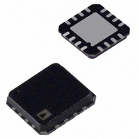
ADA4950-1YCPZ-RL Analog Devices Inc, ADA4950-1YCPZ-RL Datasheet - Page 17

ADA4950-1YCPZ-RL
Manufacturer Part Number
ADA4950-1YCPZ-RL
Description
Fixed Gain 1,2&3 Diff ADC Driver
Manufacturer
Analog Devices Inc
Datasheet
1.ADA4950-1YCPZ-R7.pdf
(28 pages)
Specifications of ADA4950-1YCPZ-RL
Amplifier Type
Differential
Number Of Circuits
1
Output Type
Differential
Slew Rate
2900 V/µs
-3db Bandwidth
750MHz
Voltage - Input Offset
200µV
Current - Supply
9.5mA
Current - Output / Channel
114mA
Voltage - Supply, Single/dual (±)
3 V ~ 11 V, ±1.5 V ~ 5.5 V
Operating Temperature
-40°C ~ 105°C
Mounting Type
Surface Mount
Package / Case
16-LFCSP
Lead Free Status / RoHS Status
Lead free / RoHS Compliant
Gain Bandwidth Product
-
Current - Input Bias
-
Lead Free Status / RoHS Status
Lead free / RoHS Compliant
TERMINOLOGY
Differential Voltage
Differential voltage refers to the difference between two node
voltages. For example, the output differential voltage (or equiv-
alently, output differential node voltage) is defined as
where V
−OUT output terminals with respect to a common ground
reference.
The input differential voltage is defined in different ways,
depending upon the selected gain.
For G = 1
where +INA and −INA refer to the voltages at the +INA and
−INA input terminals with respect to a common ground
reference (input terminals +INB and −INB are floating).
For G = 2
where +INB and −INB refer to the voltages at the +INB and
−INB input terminals with respect to a common ground
reference (input terminals +INA and −INA are floating).
For G = 3, input terminals +INA and +INB are connected
together, and input terminals −INA and −INB are connected
together.
where +INAB and −INAB refer to the voltages at the connection
of input terminals +INA and +INB and at the connection of
input terminals −INA and −INB with respect to a common
ground reference.
V
V
V
V
V
+INB
+INA
–INA
–INB
OUT, dm
IN, dm
IN, dm
IN, dm
OCM
+OUT
= (+INA − (−INA))
= (+INB − (−INB))
= (+INAB − (−INAB))
= (V
and V
250Ω
500Ω
500Ω
250Ω
R
R
R
R
GB
GA
GA
GB
Figure 52. Signal and Circuit Definitions
+OUT
−OUT
+IN
− V
–IN
refer to the voltages at the +OUT and
−OUT
ADA4950-x
)
500Ω
500Ω
R
R
F
F
–OUT
+OUT
R
L, dm
V
OUT, dm
Rev. 0 | Page 17 of 28
Common-Mode Voltage
Common-mode voltage refers to the average of two node
voltages with respect to the local ground reference. The output
common-mode voltage is defined as
Output Balance
Output balance is a measure of how close the output differential
signals are to being equal in amplitude and opposite in phase.
Any imbalances in amplitude or phase produce an undesired
common-mode signal at the amplifier output. Output balance
error is defined as the magnitude of the output common-mode
voltage divided by the magnitude of the output differential
mode voltage.
V
Output
OUT, cm
= (V
Balance
+OUT
+ V
Error
−OUT
ADA4950-1/ADA4950-2
=
)/2
Δ
Δ
V
V
OUT
OUT
,
,
cm
dm


