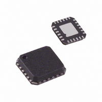
ADA4950-2YCPZ-R7 Analog Devices Inc, ADA4950-2YCPZ-R7 Datasheet - Page 8

ADA4950-2YCPZ-R7
Manufacturer Part Number
ADA4950-2YCPZ-R7
Description
Fixed Gain 1,2&3 Diff ADC Driver
Manufacturer
Analog Devices Inc
Datasheet
1.ADA4950-1YCPZ-R7.pdf
(28 pages)
Specifications of ADA4950-2YCPZ-R7
Amplifier Type
Differential
Number Of Circuits
2
Output Type
Differential
Slew Rate
2900 V/µs
-3db Bandwidth
750MHz
Voltage - Input Offset
200µV
Current - Supply
9.5mA
Current - Output / Channel
114mA
Voltage - Supply, Single/dual (±)
3 V ~ 11 V, ±1.5 V ~ 5.5 V
Operating Temperature
-40°C ~ 105°C
Mounting Type
Surface Mount
Package / Case
24-LFCSP
Lead Free Status / RoHS Status
Lead free / RoHS Compliant
Gain Bandwidth Product
-
Current - Input Bias
-
Lead Free Status / RoHS Status
Lead free / RoHS Compliant
Other names
ADA4950-2YCPZ-R7TR
Available stocks
Company
Part Number
Manufacturer
Quantity
Price
Company:
Part Number:
ADA4950-2YCPZ-R7
Manufacturer:
AD
Quantity:
3 059
ADA4950-1/ADA4950-2
PIN CONFIGURATIONS AND FUNCTION DESCRIPTIONS
Table 9. ADA4950-1 Pin Function Descriptions
Pin No.
1
2
3
4
5 to 8
9
10
11
12
13 to 16
17 (EPAD)
Table 10. ADA4950-2 Pin Function Descriptions
Pin No.
1
2
3, 4
5
6
7
8
9, 10
11
12
13
14
15, 16
17
18
19
20
21, 22
23
24
25 (EPAD)
NOTES
1. SOLDER THE EXPOSED PADDLE ON THE BACK OF
THE PACKAGE TO A GROUND PLANE OR TO A
POWER PLANE.
Mnemonic
+INB
+INA
−INA
−INB
+V
V
+OUT
−OUT
PD
−V
Exposed Paddle (EPAD)
Mnemonic
−INA1
−INB1
+V
+INB2
+INA2
−INA2
−INB2
+V
V
+OUT2
−OUT2
PD2
−V
V
+OUT1
−OUT1
PD1
−V
+INB1
+INA1
Exposed Paddle (EPAD)
OCM
OCM2
OCM1
Figure 5. ADA4950-1 Pin Configuration
S
S
S1
S2
S2
S1
+INB
+INA
–INA
–INB
1
2
3
4
ADA4950-1
(Not to Scale)
TOP VIEW
PIN 1
INDICATOR
12 PD
11 –OUT
10 +OUT
9 V
Description
Positive Input B, 250 Ω Input. Use alone for G = 2 or tie to +INA for G = 3.
Positive Input A, 500 Ω Input. Use alone for G = 1 or tie to +INB for G = 3.
Negative Input A, 500 Ω Input. Use alone for G = 1 or tie to −INB for G = 3.
Negative Input B, 250 Ω Input. Use alone for G = 2 or tie to −INA for G = 3.
Positive Supply Voltage.
Output Common-Mode Voltage.
Positive Output.
Negative Output.
Power-Down Pin.
Negative Supply Voltage.
Solder the exposed paddle on the back of the package to a ground plane or to a power plane.
Description
Negative Input A, Amplifier 1, 500 Ω Input. Use alone for G = 1 or tie to –INB1 for G = 3.
Negative Input B, Amplifier 1, 250 Ω Input. Use alone for G = 2 or tie to –INA1 for G = 3.
Positive Supply Voltage, Amplifier 1.
Positive Input B, Amplifier 2, 250 Ω Input. Use alone for G = 2 or tie to +INA2 for G = 3.
Positive Input A, Amplifier 2, 500 Ω Input. Use alone for G = 1 or tie to +INB2 for G = 3.
Negative Input A, Amplifier 2, 500 Ω Input. Use alone for G = 1 or tie to –INB2 for G = 3.
Negative Input B, Amplifier 2, 250 Ω Input. Use alone for G = 2 or tie to –INA2 for G = 3.
Positive Supply Voltage, Amplifier 2.
Output Common-Mode Voltage, Amplifier 2.
Positive Output, Amplifier 2.
Negative Output, Amplifier 2.
Power-Down Pin, Amplifier 2.
Negative Supply Voltage, Amplifier 2.
Output Common-Mode Voltage, Amplifier 1.
Positive Output, Amplifier 1.
Negative Output, Amplifier 1.
Power-Down Pin, Amplifier 1.
Negative Supply Voltage, Amplifier 1.
Positive Input B, Amplifier 1, 250 Ω Input. Use alone for G = 2 or tie to +INA1 for G = 3.
Positive Input A, Amplifier 1, 500 Ω Input. Use alone for G = 1 or tie to +INB1 for G = 3.
Solder the exposed paddle on the back of the package to a ground plane or to a power plane.
OCM
Rev. 0 | Page 8 of 28
NOTES
1. SOLDER THE EXPOSED PADDLE ON THE BACK OF
THE PACKAGE TO A GROUND PLANE OR TO A
POWER PLANE.
–INA1
–INB1
+INB2
+INA2
Figure 6. ADA4950-2 Pin Configuration
+V
+V
S1
S1
1
2
3
4
5
6
ADA4950-2
(Not to Scale)
TOP VIEW
PIN 1
INDICATOR
18
17
16
15
14
13
+OUT1
V
–V
–V
PD2
–OUT2
OCM1
S2
S2


