ADATE206BSVZ Analog Devices Inc, ADATE206BSVZ Datasheet
ADATE206BSVZ
Specifications of ADATE206BSVZ
Available stocks


Related parts for ADATE206BSVZ


ADATE206BSVZ Summary of contents
Page 1
FEATURES Driver, comparator, and active load 500 MHz toggle rate Inhibit mode function Dynamic clamps Operating voltage range: −1 6.5 V Output voltage swing: 200 Four range adjustable slew rate True/complement data mode bit ...
Page 2
ADATE206 TABLE OF CONTENTS Features .............................................................................................. 1 Applications ....................................................................................... 1 General Description ......................................................................... 1 Functional Block Diagram .............................................................. 1 Table of Contents .............................................................................. 2 Revision History ............................................................................... 2 Specifications ..................................................................................... 3 Electrical Characteristics ............................................................. 3 REVISION HISTORY 10/08— Rev. 0 ...
Page 3
SPECIFICATIONS ELECTRICAL CHARACTERISTICS = −5 10 75°C, unless otherwise noted Table 1. Parameter DRIVER Single-Ended Logic Input Characteristics (VTEN, DRV_INV) Threshold Voltage Voltage Range Bias Current Single-Ended Logic Input Characteristics ...
Page 4
ADATE206 Parameter VIT Linearity Error Offset Tempco Driver Interaction VH Interaction Interaction Interaction Interaction Interaction Interaction to VL Rise/Fall Times at Device Under Testing (DUT) ...
Page 5
Parameter Settling Time Settling Time Rise and Fall Time Temperature Coefficient 500 mV Swing 1 V Swing 3 V Swing 5 V Swing Overshoot and Preshoot 200 mV swing Overshoot and Preshoot 1 V ...
Page 6
ADATE206 Parameter Offset Gain Error Linearity Error Single-Ended Logic Input Characteristics Threshold Voltage (CLLM) Voltage Range Bias Current Bias Current Digital Output Characteristics (VOH, VOL Levels) Logic 1 Logic 0 Differential Levels COMPARATOR AC SPECIFICATIONS Propagation Delay Input to Output ...
Page 7
Parameter VDUT Range VDUT Range Output characteristics Gain Load Offset, IOH, IOL T Load Nonlinearity, IOH, IOL T Output Current Tempco, IOH, IOL T VCOM Buffer (Through Bridge) VCOM Buffer Offset VCOM Buffer Bias Current VCOM Buffer Gain VCOM Buffer ...
Page 8
ADATE206 ABSOLUTE MAXIMUM RATINGS Table 2. Parameter Maximum Current for VCC Maximum Current for VEE Positive Supply Voltage (VCC to GND) Negative Supply Voltage (VEE to GND) Operating Temperature (Junction) Storage Temperature Range ESD (Human Body Model) ESD CAUTION ESD ...
Page 9
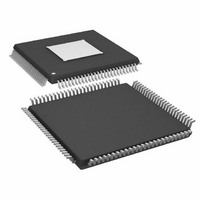
PIN CONFIGURATION AND FUNCTION DESCRIPTIONS 100 VCOM_1 1 GNDREF_1 2 VIOH_1 3 VIOL_1 4 GND 5 ...
Page 10
ADATE206 Table 3. Pin Function Descriptions Pin No. Mnemonic 1 VCOM_1 2 GNDREF_1 3 VIOH_1 4 VIOL_1 GND 5, 12, 20, 21, 36, 40, 55, 56, 64, 71, 76, 79, 83, 93, 97, 100 6 D_INV_1 7 VIT_1 8 VIL_1 ...
Page 11
Pin No. Mnemonic 47 DR_EN_N_2 48 DR_EN_N_T_2 49 DR_EN_P_T_2 50 DR_EN_P_2 51 DR_DATA_N_2 52 DR_DATA_N_T_2 53 DR_DATA_P_T_2 54 DR_DATA_P_2 61 VTEN_2 62 LDEN_2 63 CLLM_2 65 CLAMPL_2 66 CLAMPH_2 67 VIH_2 68 VIL_2 69 VIT_2 70 D_INV_2 72 VIOL_2 73 ...
Page 12
ADATE206 TYPICAL PERFORMACE CHARACTERISTICS 2400 VIH = 5V 2200 2000 VIL = 0V 1800 TERMINATION = 50Ω 1600 1400 VIH = 3V 1200 1000 800 600 400 VIH = 1V 200 2ns/DIV Figure ...
Page 13
TEMPERATURE (°C) Figure 9. Driver Gain vs. Temperature 2.0 1.5 1.0 0.5 0 –0.5 –1.0 –1 TEMPERATURE (°C) Figure 10. Driver Offset ...
Page 14
ADATE206 32.0 30.0 27.5 25.0 22.0 20.0 17.5 15.0 12.5 10.0 7.5 5.0 2.5 0 –3 1ns/DIV Figure 15. Comparator t vs. Pulse Width COM IOH = IOL = ...
Page 15
THEORY OF OPERATION The ADATE206 has two general classes of logic inputs: differential inputs for controlling functions that generally need to be operated at high speed, and single-ended CMOS inputs for setting operating modes or other low speed functions. The ...
Page 16
ADATE206 OUTLINE DIMENSIONS 0° MIN 1.05 1.00 0.95 0.15 SEATING 0.05 0.08 MAX PLANE COPLANARITY VIEW A ROTATED 90 ° CCW ORDERING GUIDE Model Temperature Range ADATE206BSV −40°C to +85°C ©2006–2008 Analog Devices, Inc. All rights reserved. Trademarks and registered ...