ADAU1445YSVZ-3A Analog Devices Inc, ADAU1445YSVZ-3A Datasheet - Page 27
ADAU1445YSVZ-3A
Manufacturer Part Number
ADAU1445YSVZ-3A
Description
175MHZ SigmaDSP,2x8 SRCs
Manufacturer
Analog Devices Inc
Series
SigmaDSP®r
Type
Audio Processorr
Datasheet
1.ADAU1446YSTZ-3A.pdf
(92 pages)
Specifications of ADAU1445YSVZ-3A
Applications
Automotive Audio
Mounting Type
Surface Mount
Package / Case
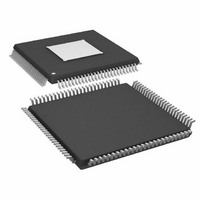
100-TQFP Exposed Pad, 100-eTQFP, 100-HTQFP, 100-VQFP
Lead Free Status / RoHS Status
Lead free / RoHS Compliant
Available stocks
Company
Part Number
Manufacturer
Quantity
Price
Company:

Part Number:
ADAU1445YSVZ-3A
Manufacturer:
Analog Devices Inc
Quantity:
10 000
Part Number:
ADAU1445YSVZ-3A
Manufacturer:
ADI/亚德诺
Quantity:
20 000
Company:
Part Number:
ADAU1445YSVZ-3A-RL
Manufacturer:
Analog Devices Inc
Quantity:
10 000


SPI Port
By default, the ADAU1445/ADAU1446 are in I
these parts can be put into SPI control mode by pulling CLATCH
low three times. Each low pulse should have a minimum duration
of 20 ns, and the delay between pulses should be at least 20 ns.
The SPI port uses a 4-wire interface, consisting of CLATCH,
CCLK, CDATA, and COUT signals. The CLATCH signal goes
low at the beginning of a transaction and high at the end of a
transaction. The CCLK signal latches CDATA on a low-to-high
transition. COUT data is shifted out of the ADAU1445/ADAU1446
on the falling edge of CCLK and should be clocked into a receiving
device, such as a microcontroller, on the next CCLK falling edge
(rising edge is possible if t
carries the serial input data, and the COUT signal is the serial
output data. The COUT signal remains three-stated until a read
operation is requested. This allows other SPI-compatible periph-
erals to share the same readback line. All SPI transactions have
the same word sequence shown in Table 13 (see Figure 4 for an
SPI port timing diagram). All data written should be MSB first.
Chip Address R/ W
The first byte of an SPI transaction includes the 7-bit chip address
and a R/ W bit. The chip address is set by the ADDR0 pin. This
allows two ADAU1445/ADAU1446 devices to share a CLATCH
Table 13. Generic Control Word Sequence
Byte 0
Chip Address[6:0], R/W
1
Continues to end of data.
CLATCH
CDATA
CCLK
CLATCH
CDATA
COUT
CCLK
COV
timing is met). The CDATA signal
BYTE 0
Byte 1
Subaddress[15:8]
HIGH-Z
BYTE 0
2
C mode, but
Figure 19. SPI Write Clocking (Single-Write Mode)
Figure 20. SPI Read Clocking (Single-Read Mode)
BYTE 1
Rev. A | Page 27 of 92
DATA
Byte 2
Subaddress[7:0]
signal, yet still operate independently. When ADDR0 is low, the
chip address is 0000000; when ADDR0 is high, the address is
0000001. The LSB of the first byte determines whether the SPI
transaction is a read (Logic Level 1) or a write (Logic Level 0).
Users can communicate with both ICs with up to five latch signals
by using the USBi communication channel list in the hardware
configuration tab in SigmaStudio.
Subaddress
The 16-bit subaddress word is decoded into a location in one of
the memories or registers. This subaddress is the location of the
appropriate RAM location or register.
Data Bytes
The number of data bytes varies according to the register or
memory being accessed. In burst write mode, an initial
subaddress is given followed by a continuous sequence of data
for consecutive memory or register locations. The detailed data
format for continuous mode operation is shown in Figure 4.
A sample timing diagram for a single SPI write operation to the
parameter RAM is shown in Figure 19. A sample timing
diagram of a single SPI read operation is shown in Figure 20.
The COUT pin goes from three-state to driven at the beginning
of Byte 3. In this example, Byte 0 to Byte 2 contain the addresses
and R/ W bit, and subsequent bytes carry the data.
BYTE 1
DATA
BYTE 2
Byte 3
Data
DATA
ADAU1445/ADAU1446
BYTE 3
HIGH-Z
Byte 4
Data
1
Related parts for ADAU1445YSVZ-3A
Image
Part Number
Description
Manufacturer
Datasheet
Request
R

Part Number:
Description:
±1.7g Dual-Axis IMEMS Accelerometer Evaluation Board
Manufacturer:
Analog Devices Inc
Datasheet:

Part Number:
Description:
Inertial Sensor Evaluation System
Manufacturer:
Analog Devices Inc
Datasheet:
Part Number:
Description:
Manufacturer:
Analog Devices Inc
Datasheet:
Part Number:
Description:
Manufacturer:
Analog Devices Inc
Datasheet:
Part Number:
Description:
Manufacturer:
Analog Devices Inc
Datasheet:
Part Number:
Description:
Manufacturer:
Analog Devices Inc
Datasheet:
Part Number:
Description:
Manufacturer:
Analog Devices Inc
Datasheet:
Part Number:
Description:
Manufacturer:
Analog Devices Inc
Datasheet:
Part Number:
Description:
Manufacturer:
Analog Devices Inc
Datasheet:
Part Number:
Description:
Manufacturer:
Analog Devices Inc
Datasheet:
Part Number:
Description:
Manufacturer:
Analog Devices Inc
Datasheet:
Part Number:
Description:
Manufacturer:
Analog Devices Inc
Datasheet:
Part Number:
Description:
Manufacturer:
Analog Devices Inc
Datasheet: