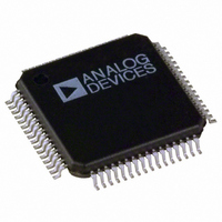
ADAV803ASTZ Analog Devices Inc, ADAV803ASTZ Datasheet - Page 56

ADAV803ASTZ
Manufacturer Part Number
ADAV803ASTZ
Description
IC,Soundcard Circuits,QFP,64PIN,PLASTIC
Manufacturer
Analog Devices Inc
Type
Audio Codecr
Datasheet
1.ADAV803ASTZ-REEL.pdf
(60 pages)
Specifications of ADAV803ASTZ
Data Interface
Serial
Resolution (bits)
24 b
Number Of Adcs / Dacs
2 / 2
Sigma Delta
No
Dynamic Range, Adcs / Dacs (db) Typ
102 / 101
Voltage - Supply, Analog
3 V ~ 3.6 V
Voltage - Supply, Digital
3 V ~ 3.6 V
Operating Temperature
-40°C ~ 85°C
Mounting Type
Surface Mount
Package / Case
64-LQFP
Adc/dac Resolution
24b
Number Of Adc's
2
Number Of Dac's
2
Interface Type
Serial (I2C)
Power Supply Type
Analog/Digital
Operating Supply Voltage (min)
3V
Operating Supply Voltage (typ)
3.3V
Operating Supply Voltage (max)
3.6V
Sample Rate
96KSPS
Pin Count
64
Operating Temperature (min)
-40C
Operating Temperature (max)
85C
Screening Level
Industrial
Package Type
LQFP
Mounting
Surface Mount
Lead Free Status / RoHS Status
Lead free / RoHS Compliant
For Use With
EVAL-ADAV803EBZ - BOARD EVALUATION FOR ADAV803
Lead Free Status / Rohs Status
Compliant
Available stocks
Company
Part Number
Manufacturer
Quantity
Price
Company:
Part Number:
ADAV803ASTZ
Manufacturer:
ADI
Quantity:
163
Company:
Part Number:
ADAV803ASTZ
Manufacturer:
Analog Devices Inc
Quantity:
10 000
Company:
Part Number:
ADAV803ASTZ-REEL
Manufacturer:
Analog Devices Inc
Quantity:
10 000
ADAV803
PLL Clock Source Register—Address 1111000 (0x78)
Table 136. PLL Clock Source Register Bit Map
7
PLL2_Source
Table 137. PLL Clock Source Register Bit Descriptions
Bit Name
PLL2_Source
PLL1_Source
PLL Output Enable—Address 1111010 (0x7A)
Table 138. PLL Output Enable Register Bit Map
7
Reserved
Table 139. PLL Output Enable Register Bit Descriptions
Bit Name
DIRINPD
DIRIN_PIN
SYSCLK1
SYSCLK2
SYSCLK3
6
PLL1_Source
6
Reserved
This bit powers down the S/PDIF receiver.
This bit determines the input levels of the DIRIN pin.
Enables the SYSCLK1 output.
Enables the SYSCLK2 output.
Enables the SYSCLK3 output.
Description
Selects the clock source for PLL2.
Selects the clock source for PLL1.
Description
0 = Normal.
1 = Power-down.
0 = DIRIN accepts input signals down to 200 mV according to AES3 requirements.
1 = DIRIN accepts input signals as defined in the Specifications section.
0 = Enabled.
1 = Disabled.
0 = Enabled.
1 = Disabled.
0 = Enabled.
1 = Disabled.
0 = XIN.
1 = MCLKI.
0 = XIN.
1 = MCLKI
5
Reserved
5
DIRINPD
4
Reserved
4
DIRIN_PIN
Rev. A | Page 56 of 60
3
Reserved
3
Reserved
2
Reserved
2
SYSCLK1
1
Reserved
1
SYSCLK2
0
Reserved
0
SYSCLK3


