ADCMP605BCPZ-WP Analog Devices Inc, ADCMP605BCPZ-WP Datasheet - Page 7
ADCMP605BCPZ-WP
Manufacturer Part Number
ADCMP605BCPZ-WP
Description
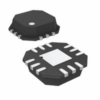
IC,VOLT COMPARATOR,SINGLE,LLCC,12PIN,PLASTIC
Manufacturer
Analog Devices Inc
Type
with Latchr
Datasheet
1.ADCMP604BKSZ-REEL7.pdf
(16 pages)
Specifications of ADCMP605BCPZ-WP
Number Of Elements
1
Output Type
Complementary, LVDS, Rail-to-Rail
Voltage - Supply
2.5 V ~ 5.5 V, ±1.25 V ~ 2.75 V
Mounting Type
Surface Mount
Package / Case
12-VFQFN, CSP Exposed Pad
No. Of Comparators
1
Ic Output Type
LVDS
Supply Current
1.6mA
Supply Voltage Range
2.5V To 5.5V
Amplifier Case Style
LFCSP
No. Of Pins
12
Operating Temperature Range
-40°C To +125°C
Lead Free Status / RoHS Status
Lead free / RoHS Compliant
Available stocks
Company
Part Number
Manufacturer
Quantity
Price
Company:

Part Number:
ADCMP605BCPZ-WP
Manufacturer:
SANYO
Quantity:
12 000
Part Number:
ADCMP605BCPZ-WP
Manufacturer:
ADI/亚德诺
Quantity:
20 000


PIN CONFIGURATION AND FUNCTION DESCRIPTIONS
Table 5. ADCMP604 Pin Function Descriptions (6-Lead SC70)
Pin No.
1
2
3
4
5
6
Table 6. ADCMP605 Pin Function Descriptions (12-Lead LFCSP_VQ)
Pin No.
1
2
3, 5, 9, 11
4
6
7
8
10
12
Heat Sink Paddle
Mnemonic
Q
V
V
V
V
Q
EE
P
N
CCI
/V
CCO
Mnemonic
V
V
V
V
V
S
LE/HYS
Q
Q
V
DN
CCO
CCI
EE
P
N
EE
Description
Noninverting Output. Q is at logic high if the analog voltage at the noninverting input, V
analog voltage at the inverting input, V
Negative Supply Voltage.
Noninverting Analog Input.
Inverting Analog Input.
Input Section Supply/Output Section Supply. V
Inverting Output. Q is at logic low if the analog voltage at the noninverting input, V
voltage at the inverting input, V
Description
Output Section Supply.
Input Section Supply.
Negative Supply Voltages.
Noninverting Analog Input.
Inverting Analog Input.
Shutdown. Drive this pin low to shut down the device.
Latch/Hysteresis Control. Bias with resistor or current for hysteresis; drive low to latch.
Inverting Output. Q is at Logic low if the analog voltage at the noninverting input, V
the analog voltage at the inverting input, V
Noninverting Output. Q is at Logic high if the analog voltage at the noninverting input, V
than the analog voltage at the inverting input, V
The metallic back surface of the package is electrically connected to V
because Pin 3, Pin 5, Pin 9, and Pin 11 provide adequate electrical connection. It can also be
soldered to the application board if improved thermal and/or mechanical stability is desired.
V
Figure 3. ADCMP604 Pin Configuration
Figure 4. ADCMP605 Pin Configuration
V
V
CCO
V
V
EE
CCI
Q
EE
P
N
1
2
3
.
1
2
3
ADCMP604
(Not to Scale)
Rev. A | Page 7 of 16
ADCMP605
TOP VIEW
(Not to Scale)
TOP VIEW
N
PIN 1
INDICATOR
.
CCI
6
5
4
and V
Q
V
V
9 V
8 LE/HYS
7 S
CCI
N
N
/V
EE
DN
, if the comparator is in compare mode.
CCO
CCO
N
are shared pin.
, if the comparator is in compare mode.
ADCMP604/ADCMP605
EE
. It can be left floating
P,
is greater than the analog
P
, is greater than the
P
, is greater than
P
, is greater
Related parts for ADCMP605BCPZ-WP
Image
Part Number
Description
Manufacturer
Datasheet
Request
R

Part Number:
Description:
±1.7g Dual-Axis IMEMS Accelerometer Evaluation Board
Manufacturer:
Analog Devices Inc
Datasheet:

Part Number:
Description:
Inertial Sensor Evaluation System
Manufacturer:
Analog Devices Inc
Datasheet:
Part Number:
Description:
Manufacturer:
Analog Devices Inc
Datasheet:
Part Number:
Description:
Manufacturer:
Analog Devices Inc
Datasheet:
Part Number:
Description:
Manufacturer:
Analog Devices Inc
Datasheet:
Part Number:
Description:
Manufacturer:
Analog Devices Inc
Datasheet:
Part Number:
Description:
Manufacturer:
Analog Devices Inc
Datasheet:
Part Number:
Description:
Manufacturer:
Analog Devices Inc
Datasheet:
Part Number:
Description:
Manufacturer:
Analog Devices Inc
Datasheet:
Part Number:
Description:
Manufacturer:
Analog Devices Inc
Datasheet:
Part Number:
Description:
Manufacturer:
Analog Devices Inc
Datasheet:
Part Number:
Description:
Manufacturer:
Analog Devices Inc
Datasheet:
Part Number:
Description:
Manufacturer:
Analog Devices Inc
Datasheet: