ADDAC80-CCD-V Analog Devices Inc, ADDAC80-CCD-V Datasheet
ADDAC80-CCD-V
Specifications of ADDAC80-CCD-V
Available stocks


Related parts for ADDAC80-CCD-V


ADDAC80-CCD-V Summary of contents
Page 1
... PRODUCT DESCRIPTION The ADDAC80 Series is a family of low cost 12-bit digital-to- analog converters with both a high stability voltage reference and output amplifier combined on a single monolithic chip. The ADDAC80 Series is recommended for all low cost 12-bit D/A converter applications where reliability and cost are of paramount importance ...
Page 2
... Max External Current Tempco of Drift POWER SUPPLY SENSITIVITY ± ± 10 supply when applicable ± ± 5% POWER SUPPLY REQUIREMENTS Rated Voltages Range Analog Supplies Logic Supplies Supply Drain +12 V, +15 V –12 V, –15 V ADDAC80 ADDAC85 Min Typ Max Min Typ Monolithic Monolithic 12 2.0 5.5 2 ...
Page 3
... ADDAC80/ADDAC85/ADDAC87 ADDAC87 Max Min Typ Max Unit °C +85 –55 +125 °C +125 –55 +125 °C +150 –65 +150 ADDAC87 Max Min Typ Max Unit ...
Page 4
... see Figure 3a Maximum with no degradation of specification, must be a constant load. 7 Including 5 mA load supply required only for CCD versions. Specifications subject to change without notice. ADDAC80 ADDAC85 Min Typ Max Min Typ ± 2.5, ± 5, ± 2.5, ± 5, ± 10, +5, ± 10, +5, ...
Page 5
... ADDAC80/ADDAC85/ADDAC87 ADDAC87 Max Min Typ Max Unit Hybrid 12 12 Bits Digits 5.5 2.0 5.5 V 0.8 0 0.8 V µA 250 µ ...
Page 6
... NETWORK 5k BIT 7 AND 7 CURRENT BIT 8 8 SWITCHES 6.3k BIT 9 9 – BIT BIT 11 11 ADDAC80 (LSB) BIT CBI VERSIONS 5V – CCD VERSIONS ADDAC85LD ADDAC85MIL Min Typ Max Min Typ ± 15, 5 ± 15, 5 ± 14.5 ± 15.5 ± 14.5 ± 15.5 +4 ...
Page 7
... Input Model Code ADDAC80N-CBI-V Binary ADDAC80D-CBI-V Binary ADDAC85D-CBI-V Binary ADDAC87D-CBI-V Binary ADDAC80-CBI-V Binary ADDAC80-CBI-I Binary ADDAC80-CCD-V Binary Coded Decimal ADDAC80-CCD-I Binary Coded Decimal 2 ADDAC80Z-CBI-V Binary 2 ADDAC80Z-CBI-I Binary 2 ADDAC80Z-CCD-V Binary Coded Decimal 2 ADDAC80Z-CCD-I Binary Coded Decimal 3 ADDAC85C-CBI-V Binary ADDAC85C-CBI-I Binary 3 ADDAC85-CBI-V Binary ...
Page 8
... FSR/°C). Gain drift is established by: 1) testing the end point differences for each ADDAC80 model at the lowest operating temperature, 25°C and the highest operating temperature; 2) calculating the gain error with respect to the 25° ...
Page 9
... A mismatch the DAC resistors is usually the largest component of bipolar drift, but in the ADDAC80 this error is held to 10 ppm/°C max. Gain drift in the DAC also contributes to bipolar offset drift, as well as full-scale drift, but again is held to 10 ppm/°C max. ...
Page 10
... ADDAC80/ADDAC85/ADDAC87 1 24 REF 2 23 CONTROL CIRCUIT 12-BIT 5 20 RESISTOR 2k LADDER 6 19 NETWORK 3k 7 AND 18 CURRENT SWITCHES 6. Offset Adjustment For unipolar (CSB) configurations, apply the digital input code that should produce zero potential output and adjust the OFFSET potentiometer for zero output. For bipolar (COB, CTC) configurations, apply the digital input code that should produce the maximum negative output voltage ...
Page 11
... Internal resistors are provided to scale an external op amp or to configure a resistive load to offer two output voltage ranges of ± –2 V. These resistors (R integral part of the ADDAC80 and maintain gain and bipolar offset drift specifications. If the internal resistors are not used, exter- nal R ( less to minimize drift. This will typically add ± ...
Page 12
... ADDAC80 output current and R OUT back resistor. Using the internal feedback resistors of the current model ADDAC80 provides output voltage ranges the same as the voltage model ADDAC80. To obtain the desired output voltage range when connecting an external op amp, refer to Table V and Figure 14. Internal ...
Page 13
... ALL LEADS — INCREASE MAXIMUM LIMIT BY 0.003" (0.08 mm) MEASURED AT THE CENTER OF THE FLAT, WHEN HOT SOLDER DIP LEAD FINISH IS APPLIED. 7. TWENTY TWO SPACES. 8. CONTROLLING DIMENSIONS ARE IN MILLIMETERS. INCH DIMENSIONS ARE ROUNDED-OFF MILLIMETER EQUIVALENTS FOR REFERENCE ONLY AND ARE NOT APPROPRIATE FOR USE IN DESIGN ADDAC80/ADDAC85/ADDAC87 Connect Connect Connect Pin 17 to ...
Page 14
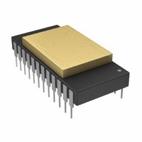
... ADDAC80/ADDAC85/ADDAC87 24-Lead Side Brazed Ceramic DIP for Hybrid (DH-24A) 0.005 (0.13) MIN 24 PIN 1 SEE NOTE 1 0.225 (5.72) MAX 0.200 (5.08) 0.120 (3.05) 0.023 (0.58) 0.014 (0.36) NOTES 1. INDEX AREA; A NOTCH OR A LEAD ONE IDENTIFICATION MARK IS LOCATED ADJACENT TO LEAD ONE. 2. THE MINIMUM LIMIT FOR DIMENSION MAY BE 0.023" (0.58 mm) FOR ALL FOUR CORNER LEADS ONLY. ...
Page 15
... Revision History Location Data Sheet changed from REV REV. B. Update OUTLINE DIMENSION drawings . . . . . . . . . . . . . . . . . . . . . . . . . . . . . . . . . . . . . . . . . . . . . . . . . . . . . . . . . . . . . . . . . . . 1 ADDAC80/ADDAC85/ADDAC87 Page ...
Page 16
...