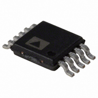
ADG1221BRMZ-REEL7 Analog Devices Inc, ADG1221BRMZ-REEL7 Datasheet - Page 5

ADG1221BRMZ-REEL7
Manufacturer Part Number
ADG1221BRMZ-REEL7
Description
IC,ANALOG SWITCH,DUAL,SPST,CMOS,TSSOP,10PIN,PLASTIC
Manufacturer
Analog Devices Inc
Series
iCMOS®r
Datasheet
1.ADG1221BRMZ.pdf
(16 pages)
Specifications of ADG1221BRMZ-REEL7
Function
Switch
Circuit
2 x SPST - NO
On-state Resistance
270 Ohm
Voltage Supply Source
Single, Dual Supply
Voltage - Supply, Single/dual (±)
10.8 V ~ 13.2 V, ±15 V
Current - Supply
1µA
Operating Temperature
-40°C ~ 85°C
Mounting Type
Surface Mount
Package / Case
10-TFSOP, 10-MSOP (0.118", 3.00mm Width)
Lead Free Status / RoHS Status
Lead free / RoHS Compliant
Parameter
DIGITAL INPUTS
DYNAMIC CHARACTERISTICS
POWER REQUIREMENTS
1
Guaranteed by design, not subject to production test.
−3 dB Bandwidth
Channel On Leakage, I
Input High Voltage, V
Input Low Voltage, V
Input Current, I
Digital Input Capacitance, C
t
t
Break-Before-Make Time Delay
(ADG1223 Only), t
Charge Injection, Q
Off Isolation
Channel-to-Channel Crosstalk
C
C
C
I
V
DD
ON
OFF
S
D
D
DD
, C
(Off )
(Off )
S
(On)
INL
or I
BBM
INJ
INL
INH
INH
D
, I
S
1
(On)
IN
25°C
±0.01
±0.2
0.001
3
190
250
120
150
70
0.2
75
90
550
2.1
2.6
2.1
2.6
3.8
4.6
0.001
140
–40°C to +85°C
±0.6
300
190
Temperature
Rev. A | Page 5 of 16
–40°C to +125°C
±1
2.0
0.8
±0.1
345
225
10
1.0
190
5/16.5
Unit
nA typ
nA max
V min
V max
μA typ
μA max
pF typ
ns typ
ns max
ns typ
ns max
ns typ
ns min
pC typ
dB typ
dB typ
MHz typ
pF typ
pF max
pF typ
pF max
pF typ
pF max
μA typ
μA max
μA typ
μA max
V min/max
ADG1221/ADG1222/ADG1223
Digital inputs = 0 V or V
Digital inputs = 5 V
Test Conditions/Comments
V
V
R
(see Figure 26)
R
(see Figure 26)
R
(see Figure 27)
V
(see Figure 28)
R
(see Figure 29)
R
(see Figure 30)
R
V
V
V
V
Digital inputs = 0 V or V
Digital inputs = 5 V
V
S
IN
L
L
L
S
L
L
L
S
S
S
DD
SS
= 300 Ω, C
= 300 Ω, C
= 300 Ω, C
= 50 Ω, C
= 50 Ω, C
= 50 Ω, C
= V
= 6 V, R
= 6 V, f = 1 MHz
= 6 V, f = 1 MHz
= 6 V, f = 1 MHz
= V
= 0 V, GND = 0 V
= 13.2 V
D
INL
= 1 V or 10 V (see Figure 25)
or V
S
= 0 Ω, C
L
L
L
INH
L
L
L
=1 pF, f = 1 MHz
= 1 pF, f = 1 MHz
= 1 pF (see Figure 31)
= 35 pF, V
= 35 pF, V
= 35 pF, V
L
= 1 nF
DD
DD
S
S
S1
= 8 V
= 8 V
= V
S2
= 8 V


