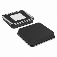
ADG2188YCPZ-HS-RL7 Analog Devices Inc, ADG2188YCPZ-HS-RL7 Datasheet - Page 20

ADG2188YCPZ-HS-RL7
Manufacturer Part Number
ADG2188YCPZ-HS-RL7
Description
IC,ANALOG SWITCH,SINGLE,8X8 CROSSPOINT,CMOS,LLCC,32PIN,PLASTIC
Manufacturer
Analog Devices Inc
Series
I²Cr
Datasheet
1.ADG2188YCPZ-HS-RL7.pdf
(28 pages)
Specifications of ADG2188YCPZ-HS-RL7
Function
Crosspoint Switch
Circuit
1 x 8:8
On-state Resistance
50 Ohm
Voltage Supply Source
Single Supply
Voltage - Supply, Single/dual (±)
12V, 15V
Current - Supply
.05µA
Operating Temperature
-40°C ~ 125°C
Mounting Type
Surface Mount
Package / Case
32-VFQFN, CSP Exposed Pad
Lead Free Status / RoHS Status
Lead free / RoHS Compliant
For Use With
EVAL-ADG2188EBZ - BOARD EVAL FOR ADG2188
Lead Free Status / RoHS Status
Lead free / RoHS Compliant
Other names
ADG2188YCPZ-HS-RL7TR
Available stocks
Company
Part Number
Manufacturer
Quantity
Price
Company:
Part Number:
ADG2188YCPZ-HS-RL7
Manufacturer:
Maxim
Quantity:
101
ADG2188
WRITING TO THE ADG2188
INPUT SHIFT REGISTER
The input shift register is 24 bits wide. A 3-byte write is necessary when writing to this register and is done under the control of the serial
clock input, SCL. The contents of the three bytes of the input shift register are shown in Figure 33 and described in Table 6.
Table 6. Input Shift Register Bit Function Descriptions
Bit
DB23 to DB17
DB16
DB15
DB14 to DB11
DB10 to DB8
DB7 to DB1
DB0
As shown in Table 6, Bit DB11 to Bit DB14 control the X input/output lines, while Bit DB8 to Bit DB10 control the Y input/output lines.
Table 7 shows the truth table for these bits. Note that the full coding sequence is written out for Channel Y0, and Channel Y1 to Channel Y7
follow a similar pattern. Note also that the RESET pin must be high when writing to the device.
Table 7. Address Decode Truth Table
DB15
DATA
1
0
1
0
1
0
1
0
1
0
1
0
X
X
1
0
1
0
X
X
DB23 (MSB)
1
DB14
AX3
0
0
0
0
0
0
0
0
0
0
0
0
0
0
1
1
1
1
1
1
1
DEVICE ADDRESS
1
Mnemonic
1110xxx
R/W
Data
AX3 to AX0
AY2 to AY0
X
LDSW
0
DB13
AX2
0
0
0
0
0
0
0
0
1
1
1
1
1
1
0
0
0
0
0
0
A2
A1
DB12
AX1
0
0
0
0
1
1
1
1
0
0
0
0
1
1
0
0
0
0
1
1
DB16 (LSB)
A0
R/W
Description
The MSBs of the ADG2188 are set to 1110. The LSBs of the address byte are set by the
state of the three address pins, Pin A0, Pin A1, and Pin A2.
Controls whether the ADG2188 slave device is read from or written to.
If R/W = 1, the ADG2188 is being read from.
If R/W = 0, the ADG2188 is being written to.
Controls whether the switch is to be open (off ) or closed (on).
If Data = 0, the switch is open/off.
If Data = 1, the switch is closed/on.
Controls I/Os X0 to X7. See Table 7 for the decode truth table.
Controls I/Os Y0 to Y7. See Table 7 for the decode truth table.
Don’t care.
This bit is useful when a number of switches need to be updated simultaneously.
If LDSW = 1, the switch position changes after the new word is read in.
If LDSW = 0, the input data is latched, but the switch position is not changed.
DB11
AX0
0
0
1
1
0
0
1
1
0
0
1
1
0
1
0
0
1
1
0
1
DB15 (MSB)
DATA AX3 AX2 AX1 AX0 AY2 AY1 AY0
DB10
AY2
0
0
0
0
0
0
0
0
0
0
0
0
0
0
0
0
0
0
0
0
Figure 33. Data-Words
Rev. 0 | Page 20 of 28
DATA BITS
DB9
AY1
0
0
0
0
0
0
0
0
0
0
0
0
0
0
0
0
0
0
0
0
DB8 (LSB)
0
0
0
0
0
0
0
0
DB8
AY0
0
0
0
0
0
0
0
0
0
0
0
0
DB7 (MSB)
X
Switch Configuration
X0 to Y0 (on)
X0 to Y0 (off )
X1 to Y0 (on)
X1 to Y0 (off )
X2 to Y0 (on)
X2 to Y0 (off )
X3 to Y0 (on)
X3 to Y0 (off )
X4 to Y0 (on)
X4 to Y0 (off )
X5 to Y0 (on)
X5 to Y0 (off )
Reserved
Reserved
X6 to Y0 (on)
X6 to Y0 (off )
X7 to Y0 (on)
X7 to Y0 (off )
Reserved
Reserved
X
X
DATA BITS
X
X
X
X
DB0 (LSB)
LDSW


