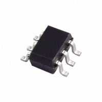
ADG3248BKSZ-REEL7 Analog Devices Inc, ADG3248BKSZ-REEL7 Datasheet

ADG3248BKSZ-REEL7
Specifications of ADG3248BKSZ-REEL7
ADG3248BKSZ-REEL7TR
Available stocks
Related parts for ADG3248BKSZ-REEL7
ADG3248BKSZ-REEL7 Summary of contents
Page 1
FEATURES 225 ps propagation delay through the switch 4.5 Ω switch connection between ports Data rate 1.244 Gbps 2.5 V/3.3 V supply operation Level translation 3 2 1.8 V Small signal bandwidth 610 MHz ...
Page 2
ADG3248 TABLE OF CONTENTS Features .............................................................................................. 1 Applications....................................................................................... 1 General Description ......................................................................... 1 Functional Block Diagram .............................................................. 1 Product Highlights ........................................................................... 1 Revision History ............................................................................... 2 Specifications..................................................................................... 3 Absolute Maximum Ratings............................................................ 4 ESD Caution.................................................................................. 4 REVISION HISTORY 10/07—Rev ...
Page 3
SPECIFICATIONS 3.6 V, GND = 0 V, all specifications T CC Table 2. Parameter DC ELECTRICAL CHARACTERISTICS Input High Voltage Input Low Voltage Input Leakage Current Off State Leakage Current On State Leakage Current Maximum ...
Page 4
ADG3248 ABSOLUTE MAXIMUM RATINGS T = 25°C, unless otherwise noted. A Table 3. Parameter V to GND CC Digital Inputs to GND DC Input Voltage DC Output Current Operating Temperature Range Industrial (B Version) Storage Temperature Range Junction Temperature θ ...
Page 5
PIN CONFIGURATION AND FUNCTION DESCRIPTIONS Table 4. Pin Function Descriptions Pin No. Mnemonic GND ADG3248 GND V 2 TOP VIEW 5 CC (Not to ...
Page 6
ADG3248 TYPICAL PERFORMANCE CHARACTERISTICS 25° 0.5 1.0 1 Figure 3. On Resistance vs. Input Voltage 25° ...
Page 7
T = 25° 2.5 2.0 1 2.5V CC 1.0 0 0.02 0.04 0.06 I (A) O Figure 9. Output Low Characteristic 3 25° ...
Page 8
ADG3248 2. 3. –40 – TEMPERATURE (°C) Figure 15. Transition Time vs. Temperature 100 1.5V p-p A 20dB ...
Page 9
TERMINOLOGY V CC Positive power supply voltage. GND Ground (0 V) reference. V INH Minimum input voltage for Logic 1. V INL Maximum input voltage for Logic Input leakage current at the control inputs Off ...
Page 10
ADG3248 BUS SWITCH APPLICATIONS MIXED VOLTAGE OPERATION, LEVEL TRANSLATION Bus switches can provide an ideal solution for interfacing between mixed voltage systems. The ADG3248 is suitable for applications in which voltage translation from 3.3 V technology to a lower voltage ...
Page 11
MULTIPLEXING Many systems, such as docking stations and memory banks, have a large number of common bus signals. Common problems faced by designers of these systems include • Large delays caused by capacitive loading of the bus • Noise due ...
Page 12
... ADG3248BKS-REEL −40°C to +85°C ADG3248BKS-REEL7 −40°C to +85°C 1 ADG3248BKSZ-REEL7 −40°C to +85° RoHS Compliant Part. ©2003–2007 Analog Devices, Inc. All rights reserved. Trademarks and registered trademarks are the property of their respective owners. D04404-0-10/07(A) 2 ...


