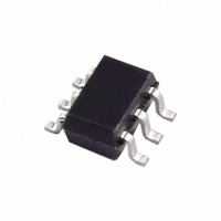
ADG742BKSZ-REEL7 Analog Devices Inc, ADG742BKSZ-REEL7 Datasheet - Page 10

ADG742BKSZ-REEL7
Manufacturer Part Number
ADG742BKSZ-REEL7
Description
IC,ANALOG SWITCH,SINGLE,SPST,CMOS,TSSOP,6PIN,PLASTIC
Manufacturer
Analog Devices Inc
Datasheet
1.ADG742BKSZ-REEL.pdf
(12 pages)
Specifications of ADG742BKSZ-REEL7
Function
Switch
Circuit
1 x SPST- NO
On-state Resistance
3 Ohm
Voltage Supply Source
Single Supply
Voltage - Supply, Single/dual (±)
1.8 V ~ 5.5 V
Operating Temperature
-40°C ~ 85°C
Mounting Type
Surface Mount
Package / Case
6-TSSOP, SC-88, SOT-363
Lead Free Status / RoHS Status
Lead free / RoHS Compliant
ADG741/ADG742
APPLICATIONS INFORMATION
The ADG741/ADG742 belong to Analog Devices’ family of
CMOS switches. This series of general-purpose switches offers
improved switching times, lower on resistance, higher
bandwidth, low power consumption, and low leakage currents.
SUPPLY VOLTAGES
Functionality of the ADG741/ADG742 extends from 1.8 V to
5.5 V single supply, which makes them ideal for battery-
powered instruments where important design parameters are
power, efficiency, and performance.
It is important to note that the supply voltage affects the input
signal range, the on resistance, and the switching times of the
part. By looking at the typical performance characteristics and
the specifications, the effects of the power supplies can be
clearly seen.
For V
temperature range.
ON RESPONSE VS. FREQUENCY
Figure 18 illustrates the parasitic components that affect the
ac performance of CMOS switches (the switch is shown
surrounded by a box). Additional external capacitances will
further degrade some performance. These capacitances affect
feedthrough, crosstalk, and system bandwidth.
The transfer function that describes the equivalent diagram of
the switch (Figure 18) is of the form A(s), as shown below.
where:
V
Figure 18. Switch Represented by Equivalent Parasitic Components
IN
C
A
R
DD
T
( )
T
S
s
= 1.8 V operation, R
=
=
=
R
C
R
LOAD
LOAD
T
⎡
⎢
⎣
s
s
(
+
(
R
(
R
R
C
R
C
ON
ON
DS
LOAD
ON
D
C
+
C
T
C
+
DS
C
D
R
DS
R
T
)
ON
)
+
ON
+
1
is typically 40 Ω over the
1
)
⎤
⎥
⎦
C
LOAD
D
R
LOAD
V
OUT
Rev. A | Page 10 of 12
The signal transfer characteristic is dependent on the switch
channel capacitance, C
zero in the numerator of the transfer function A(s). Because the
switch on resistance is small, this zero usually occurs at high
frequencies. The bandwidth is a function of the switch output
capacitance combined with C
frequency pole corresponding to these capacitances appears in
the denominator of A(s).
The dominant effect of the output capacitance, C
pole breakpoint frequency to occur first. To maximize
bandwidth, a switch must have a low input and output
capacitance and low on resistance. The on response vs.
frequency is shown in Figure 10.
OFF ISOLATION
Off isolation is a measure of the input signal coupled through
an off switch to the switch output. The capacitance, C
the input signal to the output load when the switch is off, as
shown in Figure 19.
The larger the value of C
that will be produced. The typical performance characteristic
graph of Figure 9 illustrates the drop in off isolation as a
function of frequency. From dc to roughly 1 MHz, the switch
shows better than −75 dB isolation. Up to frequencies of
10 MHz, the off isolation remains better than −55 dB. As the
frequency increases, more and more of the input signal is
coupled through to the output. Off isolation can be maximized
by choosing a switch with the smallest C
of load resistance and capacitance affect off isolation also, as
they contribute to the coefficients of the poles and zeros in the
transfer function of the switch when open.
V
IN
A
S
( )
s
=
⎡
⎢
⎣
s
Figure 19. Off Isolation Affected by External
(
s
R
(
LOAD
R
Load Resistance and Capacitance
LOAD
C
DS
) ( )
DS
C
C
. This capacitance creates a frequency
DS
C
T
DS
D
, the larger the value of feedthrough
+
)
DS
1
⎤
⎥
⎦
and the load capacitance. The
C
LOAD
D
DS
possible. The values
R
LOAD
D
, causes the
DS
, couples
V
OUT


