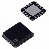
ADL5534ACPZ-R7 Analog Devices Inc, ADL5534ACPZ-R7 Datasheet - Page 13

ADL5534ACPZ-R7
Manufacturer Part Number
ADL5534ACPZ-R7
Description
Dual 5531
Manufacturer
Analog Devices Inc
Datasheet
1.ADL5534ACPZ-R7.pdf
(16 pages)
Specifications of ADL5534ACPZ-R7
Design Resources
Interfacing ADL5534 to AD9640 High Speed ADC (CN0049)
Current - Supply
98mA ~ 110mA
Frequency
20MHz ~ 500MHz
Gain
19dB ~ 20.5dB
Noise Figure
3dB
P1db
20.4dBm
Package / Case
16-VQFN, 16-CSP, Exposed Pad
Rf Type
General Purpose
Test Frequency
380MHz
Voltage - Supply
4.75 V ~ 5.25 V
Lead Free Status / RoHS Status
Lead free / RoHS Compliant
Other names
ADL5534ACPZ-R7TR
EVALUATION BOARD
Figure 23 shows the schematic for the ADL5534 evaluation
board. The board is powered by a single 5 V supply. The
components used on the board are listed in Table 6.
Transformers (T1 and T2) are provided so the ADL5534
can be configured as a balanced amplifier. Applying 5 V to
Table 6. Evaluation Board Configuration Options
Component
C1, C2, C3, C4
C5, C6
C11, C12, C13, C14,
C15, C16
C9, C10
C7, C8
R1, R2, R3, R4, R5,
R6, R7, R8
T1, T2
L1, L2
VPOS, GND,
VPOS1, GND1
W1, W2
W3
RFIN1
RFIN2
OPEN
OPEN
Description
AC coupling capacitors
Provides decoupling for the on-board linearizer
Optional components used for configuring ADL5534 as a balanced amplifier
Power-supply decoupling capacitors
Power-supply decoupling capacitors
Optional components used for configuring ADL5534 as a balanced amplifier
T1 and T2 are 50 Ω to100 Ω impedance transformers used to configure the ADL5534
as a balanced amplifier; T1 and T2 are used to present a 100 Ω differential impedance
to the ADL5534
DC bias inductor
Clip-on terminals for power supply
2-pin jumper for connection of ground and supply via cable
2-pin jumper used to connect VPOS to VPOS1
R5
R7
OPEN
OPEN
R1
R3
ADT2-1T-1P+
10nF
10nF
C1
C3
T1
1
C11
OPEN
C12
OPEN
V
POS
C15
OPEN
Figure 23. Evaluation Board Schematic
1
2
3
4
W3
NC
NC
NC
NC
Rev. 0 | Page 13 of 16
ADL5534
1nF
C6
V
Z1
POS1
470nH
470nH
NC
NC
NC
VPOS biases the amplifier corresponding to RFIN1 and
RFOUT1. Applying 5 V to VPOS1 biases the amplifier
corresponding to RFIN2 and RFOUT2. To bias both amplifiers
from a single supply, connect 5 V to VPOS or VPOS1 and
attach a jumper across W3.
L1
L2
12
11
10
9
C8
10nF
1nF
C5
C7
10nF
OPEN
C16
C10
1µF
C9
1µF
C13
OPEN
C14
OPEN
W2
VPOS1
GND1
T2
ADT2-1T-1P+
1
W1
VPOS
GND
10nF
10nF
OPEN
OPEN
C4
C2
R2
R4
OPEN
OPEN
R6
R8
Default Condition
10 nF, Size 0402
1 nF, Size 0603
Open, Size 0402
1 μF, Size 0603
10 nF, Size 0603
Open, Size 0603
Installed (Mini-Circuits®
ADT2-1T-1P+)
470 nH, Size 1008
VPOS, VPOS1; red
GND, GND1; black
W1, W2
W3
RFOUT1
RFOUT2
ADL5534


