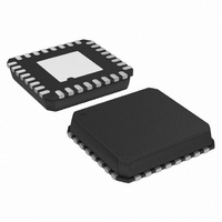
ADN2847ACPZ-32 Analog Devices Inc, ADN2847ACPZ-32 Datasheet - Page 7

ADN2847ACPZ-32
Manufacturer Part Number
ADN2847ACPZ-32
Description
IC,Laser Diode/LED Driver,LLCC,32PIN,PLASTIC
Manufacturer
Analog Devices Inc
Type
Laser Diode Driver (Fiber Optic)r
Datasheet
1.ADN2847ACPZ-32-RL.pdf
(16 pages)
Specifications of ADN2847ACPZ-32
Data Rate
3.3Gbps
Number Of Channels
1
Voltage - Supply
3 V ~ 3.6 V
Current - Supply
50mA
Current - Modulation
80mA
Current - Bias
100mA
Operating Temperature
-40°C ~ 85°C
Package / Case
32-VFQFN, CSP Exposed Pad
Mounting Type
Surface Mount
Package
32LFCSP EP
Number Of Channels Per Chip
1
Operating Supply Voltage
3 to 3.6 V
Lead Free Status / RoHS Status
Lead free / RoHS Compliant
Available stocks
Company
Part Number
Manufacturer
Quantity
Price
Part Number:
ADN2847ACPZ-32/48
Manufacturer:
ADI/亚德诺
Quantity:
20 000
PIN CONFIGURATIONS AND FUNCTION DESCRIPTIONS
Table 5. Pin Function Descriptions
48-Lead
1
2
3
4
5
6
7
8
9
10
11
12
13
14
15
16
17
18
19
20
21
22
23
24
25
26
27
28
29
30
Pin Number
IMPDMON2 9
IMPDMON 8
LBWSET 2
IMPD2 10
ERSET 4
GND4 11
V
ASET 3
PSET 5
IMPD 7
CC
TP1 1
TP2 6
4 12
N/A
1
2
3
4
N/A
5
6
N/A
N/A
7
8
9
10
N/A
11
N/A
12
13
14
15
16
N/A
N/A
N/A
17
18
19
20
21
32-Lead
Figure 7. 48-Lead LFCSP
PIN 1
INDICATOR
ADN2847
TOP VIEW
Mnemonic
TP1
LBWSET
ASET
ERSET
PSET
TP2
IMPD
IMPDMON
IMPDMON2
IMPD2
GND4
V
ERCAP
PAVCAP
TP3
V
GND1
DATAN
DATAP
GND1
CLKP
CLKN
TP4
TP5
TP6
CLKSEL
DEGRADE
FAIL
ALS
V
CC
CC
CC
4
1
3
36 GND2
35 IDTONE
34 GND2
33 IBMON
32 IMMON
31 GND3
30 V
29 ALS
28 FAIL
27 DEGRADE
26 CLKSEL
25 TP6
Test Pin. In normal operation, TP1 = GND.
Select Low Loop Bandwidth.
Alarm Current Threshold Setting Pin.
Extinction Ratio Set Pin.
Average Optical Power Set Pin.
Test Pin. In normal operation, TP2 = GND.
Monitor Photodiode Input.
Mirrored Current from Monitor Photodiode.
Mirrored Current from Monitor Photodiode 2. (For use with two MPDs).
Monitor Photodiode Input 2. (For use with two MPDs).
Supply Ground.
Supply Voltage.
Extinction Ratio Loop Capacitor.
Average Power Loop Capacitor.
Test Pin. In normal operation, TP3 = GND.
Supply Voltage.
Supply Ground.
Data, Negative Differential Terminal.
Data, Positive Differential Terminal.
Supply Ground.
Data Clock Positive Differential Terminal. Used if CLKSEL = V
Data Clock Negative Differential Terminal. Used if CLKSEL = V
Test Pin. In normal operation, TP4 = GND.
Test Pin. In normal operation, TP5 = GND.
Test Pin. In normal operation, TP6 = GND.
Clock Select. Active = V
Degrade Alarm Output.
Fail Alarm Output.
Automatic Laser Shutdown.
Supply Voltage.
Description
CC
3
Rev. A | Page 7 of 16
CC
. Used if data is clocked into chip.
IMPDMON 6
LBWSET 1
ERSET 3
GND4 7
ASET 2
PSET 4
IMPD 5
V
CC
4 8
Figure 8. 32-Lead LFCSP
ADN2847
PIN 1
INDICATOR
TOP VIEW
CC
CC
.
.
24 IBMON
23 IMMON
22 GND3
21 V
20 ALS
19 FAIL
18 DEGRADE
17 CLKSEL
CC
3
ADN2847


