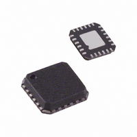
ADN8810ACPZ Analog Devices Inc, ADN8810ACPZ Datasheet - Page 12

ADN8810ACPZ
Manufacturer Part Number
ADN8810ACPZ
Description
Tunable Laser Controller
Manufacturer
Analog Devices Inc
Datasheet
1.ADN8810ACPZ-REEL7.pdf
(16 pages)
Specifications of ADN8810ACPZ
Function
Current Source (12 Bit)
Current - Output
300mA
Operating Temperature
-40°C ~ 85°C
Mounting Type
Surface Mount
Package / Case
24-LFCSP
Lead Free Status / RoHS Status
Lead free / RoHS Compliant
Voltage - Input
-
Accuracy
-
Sensing Method
-
Lead Free Status / Rohs Status
Compliant
Available stocks
Company
Part Number
Manufacturer
Quantity
Price
Company:
Part Number:
ADN8810ACPZ
Manufacturer:
SPATIION
Quantity:
27
Part Number:
ADN8810ACPZ
Manufacturer:
ADI/亚德诺
Quantity:
20 000
ADN8810
DAC to be updated. Up to eight ADN8810 devices with unique
addresses can be driven from the same serial data bus.
Table 5 shows how the 16-bit DATA input word is divided into
an address byte and a data byte. The first four bits in the input
Table 5. Serial Data Input Examples
SDI Input
Ex. 1
Ex. 2
Ex. 3
Example 1: This SDI input sets the device with an address of
111 to its minimum output current, 0 A. Connecting the
ADN8810 pins ADDR2, ADDR1, and ADDR0 to VDD sets this
address.
Example 2: This input sets the device with an address of 000 to
a current equal to half of the full-scale output.
Example 3: The ADN8810 with an address of 100 is set to full-
scale output.
STANDBY AND RESET MODES
Applying a logic low to the SB pin deactivates the ADN8810
and puts the output into a high impedance state. The device
continues to draw 1.3 mA of typical supply current in standby.
Once logic high is reasserted on the SB pin, the output current
returns to its previous value within 6 µs.
Applying logic low to RESET will set the ADN8810 data register
to all zeros, bringing the output current to 0 A. Once
deasserted, the data register can be reloaded. Data cannot be
loaded into the device while it is in Standby or Reset mode.
POWER DISSIPATION
The power dissipation of the ADN8810 is equal to the output
current multiplied by the voltage drop from PVDD to the
output.
The power dissipated by the ADN8810 will cause a temperature
increase in the device. For this reason, PVDD should be as low
as possible to minimize power dissipation.
While in operation, the ADN8810 die temperature, also known
as junction temperature, must remain below 150°C to prevent
damage. The junction temperature is approximately
where T
thermal resistance of the package (32°C/W).
T
P
DISS
J
=
T
=
A
I
+
A
OUT
is the ambient temperature in °C, and θ
θ
JA
×
×
(
PVDD
P
DISS
Address Byte
A3
0
0
0
−
V
OUT
)
−
A2
1
0
1
I
OUT
²
×
A1
1
0
0
R
S
A0
1
0
0
(3)
JA
is the
Data Byte
D11
0
1
1
RESET is
(4)
Rev. A | Page 12 of 16
D10
0
0
1
D9
0
0
1
word correspond to the address. Note that the first bit loaded
(A3) must always be zero. The remaining bits set the 12-bit data
byte for the DAC output. Three example inputs are
demonstrated.
Example 4: A 300 mA full-scale output current is required to
drive a laser diode within an 85°C environment. The laser diode
has a 2 V drop and PVDD is 3.3 V.
Using Equation 3, the power dissipation in the ADN8810 is
found to be 267 mW. At T
temperature 93.5°C, which is well below the 150°C limit. Note
that even with PVDD set to 5 V, the junction temperature
would increase to only 110°C.
USING MULTIPLE ADN8810
OUTPUT CURRENT
Connect multiple ADN8810 devices in parallel to increase the
available output current. Each device can deliver up to 300 mA
of current. To program all parallel devices simultaneously, set all
device addresses to the same address byte and drive all CS
and CLK from the same serial data interface bus. The circuit in
Figure 18 uses two ADN8810 devices and delivers 600 mA to
the pump laser.
ADDING DITHER TO THE OUTPUT CURRENT
Some tunable laser applications require the laser diode bias
current to be modulated or dithered. This is accomplished by
dithering the V
demonstrates one method.
INTERFACE
(FROM µC
OR DSP)
D8
0
0
1
SERIAL
Figure 18. Using Multiple Devices for Additional Output Current
D7
0
0
1
REF
D6
0
0
1
voltage input to the ADN8810. Figure 19
ADDR2 ADDR1
ADDR2 ADDR1
CS
SCLK
SDI
CS
SCLK
SDI
ADN8810
ADN8810
D5
0
0
1
A
= 85°C, this makes the junction
D4
0
0
1
ADDR0
ADDR0
IOUT
IOUT
R
R
FB
FB
S
SN
SN
FOR ADDITIONAL
D3
0
0
1
1.37Ω
R
1.37Ω
1.37Ω
R
1.37Ω
R
S
R
S
S
S
D2
0
0
1
D1
D1
0
0
1
I
LD
600mA
, SDI,
D0
0
0
1


