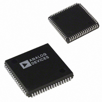
ADSP-2104BPZ-80 Analog Devices Inc, ADSP-2104BPZ-80 Datasheet - Page 7

ADSP-2104BPZ-80
Manufacturer Part Number
ADSP-2104BPZ-80
Description
5V FXD-PT DSP 20MHZ 768 WORDS RAM 68PLCC
Manufacturer
Analog Devices Inc
Series
ADSP-21xxr
Type
Fixed Pointr
Datasheet
1.ADSP-2104BPZ-80.pdf
(36 pages)
Specifications of ADSP-2104BPZ-80
Interface
Synchronous Serial Port (SSP)
Clock Rate
20MHz
Non-volatile Memory
External
On-chip Ram
1.5kB
Voltage - I/o
5.00V
Voltage - Core
5.00V
Operating Temperature
-40°C ~ 85°C
Mounting Type
Surface Mount
Package / Case
68-PLCC
Device Core Size
16b
Architecture
Enhanced Harvard
Format
Fixed Point
Clock Freq (max)
20MHz
Mips
20
Device Input Clock Speed
20MHz
Ram Size
512Byte
Program Memory Size
8KB
Operating Temp Range
-40C to 85C
Operating Temperature Classification
Industrial
Mounting
Surface Mount
Pin Count
68
Package Type
PLCC
Lead Free Status / RoHS Status
Lead free / RoHS Compliant
Lead Free Status / RoHS Status
Lead free / RoHS Compliant
Available stocks
Company
Part Number
Manufacturer
Quantity
Price
Company:
Part Number:
ADSP-2104BPZ-80
Manufacturer:
Analog Devices Inc
Quantity:
10 000
REV. 0
Program Memory Maps
Program memory can be mapped in two ways, depending on
the state of the MMAP pin. Figure 4 shows the ADSP-2104
program memory maps. Figure 5 shows the program memory
maps for the ADSP-2109.
ADSP-2104
When MMAP = 0, on-chip program memory RAM occupies
512 words beginning at address 0x0000. Off-chip program
memory uses the remaining 14K words beginning at address
0x0800. In this configuration–when MMAP = 0–the boot
loading sequence (described below in “Boot Memory Inter-
face”) is automatically initiated when RESET is released.
When MMAP = 1, 14K words of off-chip program memory
begin at address 0x0000 and on-chip program memory RAM is
located in the 512 words between addresses 0x3800–0x39FF. In
this configuration, program memory is not booted although it
can be written to and read under program control.
Figure 4. ADSP-2104 Program Memory Maps
Figure 5. ADSP-2109 Program Memory Maps
INTERNAL RAM
BOOT MEMORY
LOADED FROM
RESERVED
EXTERNAL
RESERVED
INTERNAL
512 WORDS
EXTERNAL
EXTERNAL
MMAP=0
MMAP=0
ROM
12K
1.5K
14K
4K
0x0000
0x0FF0
0x0FFF
0x1000
0x3FFF
0x0000
0x01FF
0x0200
0x07FF
0x0800
0x3FFF
INTERNAL RAM
RESERVED
RESERVED
No Booting
EXTERNAL
EXTERNAL
INTERNAL
EXTERNAL
512 WORDS
INTERNAL
MMAP=1
MMAP=1
ROM
14K
ROM
1.5K
10K
2K
2K
2K
0x0000
0x07FF
0x0800
0x0FF0
0x0FFF
0x1000
0x37FF
0x3800
0x3FFF
0x39FF
0x3A00
0x0000
0x37FF
0x3800
0x3FFF
–7–
Data Memory Interface
The data memory address bus (DMA) is 14 bits wide. The
bidirectional external data bus is 24 bits wide, with the upper 16
bits used for data memory data (DMD) transfers.
The data memory select (DMS) signal indicates access to data
memory and can be used as a chip select signal. The write (WR)
signal indicates a write operation and can be used as a write
strobe. The read (RD) signal indicates a read operation and can
be used as a read strobe or output enable signal.
The ADSP-2104/ADSP-2109 processors support memory-
mapped I/O, with the peripherals memory-mapped into the data
memory address space and accessed by the processor in the
same manner as data memory.
Data Memory Map
ADSP-2104
On-chip data memory RAM resides in the 256 words beginning
at address 0x3800, also shown in Figure 6. Data memory
locations from 0x3900 to the end of data memory at 0x3FFF
are reserved. Control and status registers for the system, timer,
wait-state configuration, and serial port operations are located in
this region of memory.
The remaining 14K of data memory is located off-chip. This
external data memory is divided into five zones, each associated
with its own wait-state generator. This allows slower peripherals
to be memory-mapped into data memory for which wait states
are specified. By mapping peripherals into different zones, you
can accommodate peripherals with different wait-state require-
ments. All zones default to seven wait states after RESET.
CONTROL REGISTERS
MEMORY-MAPPED
Figure 6. Data Memory Map
& RESERVED
10K EXTERNAL
1K EXTERNAL
1K EXTERNAL
1K EXTERNAL
1K EXTERNAL
256 WORDS
DWAIT0
DWAIT1
DWAIT3
DWAIT4
DWAIT2
ADSP-2104/ADSP-2109
0x3900
0x3C00
0x0000
0x0400
0x0800
0x3000
0x3400
0x3FFF
0x3800
EXTERNAL
INTERNAL
RAM
RAM


