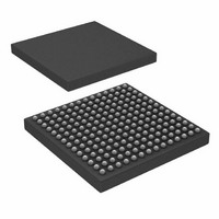
ADSP-21065LKCAZ264 Analog Devices Inc, ADSP-21065LKCAZ264 Datasheet - Page 30

ADSP-21065LKCAZ264
Manufacturer Part Number
ADSP-21065LKCAZ264
Description
ADSP-21065L 66MHZ MINI BGA
Manufacturer
Analog Devices Inc
Series
SHARC®r
Type
Fixed/Floating Pointr
Datasheet
1.ADSP-21065LKSZ-240.pdf
(44 pages)
Specifications of ADSP-21065LKCAZ264
Interface
Host Interface, Serial Port
Clock Rate
60MHz
Non-volatile Memory
External
On-chip Ram
64kB
Voltage - I/o
3.30V
Voltage - Core
3.30V
Operating Temperature
0°C ~ 85°C
Mounting Type
Surface Mount
Package / Case
196-CSPBGA
Device Core Size
32b
Architecture
Enhanced Harvard
Format
Floating Point
Clock Freq (max)
66MHz
Mips
66
Device Input Clock Speed
66MHz
Ram Size
68KB
Program Memory Size
Not RequiredKB
Operating Supply Voltage (typ)
3.3V
Operating Supply Voltage (min)
3.13V
Operating Supply Voltage (max)
3.6V
Operating Temp Range
0C to 85C
Operating Temperature Classification
Commercial
Mounting
Surface Mount
Pin Count
196
Package Type
CSPBGA
Lead Free Status / RoHS Status
Lead free / RoHS Compliant
Lead Free Status / RoHS Status
Lead free / RoHS Compliant
Available stocks
Company
Part Number
Manufacturer
Quantity
Price
Company:
Part Number:
ADSP-21065LKCAZ264
Manufacturer:
Analog Devices Inc
Quantity:
10 000
ADSP-21065L
SDRAM Interface—Bus Master
Use these specifications for ADSP-21065L bus master accesses of SDRAM.
Parameter
Timing Requirements:
t
t
Switching Characteristics:
t
t
t
t
t
t
t
t
t
t
t
t
t
NOTES
1
2
SDRAM Interface—Bus Slave
These timing requirements allow a bus slave to sample the bus master’s SDRAM command and detect when a refresh occurs.
Parameter
Timing Requirements:
t
t
t
t
NOTE
*Command = SDCKE, RAS, CAS, and SDWE.
Command = SDCKE, MSx, RAS, CAS, SDWE, DQM, and SDA10.
SDRAM controller adds one SDRAM CLK three-stated cycle delay (t
SDSDK
HDSDK
DSDK1
DSDK2
SDK
SDKH
SDKL
DCADSDK
HCADSDK
SDTRSDK
SDENSDK
SDCTR
SDCEN
SDATR
SDAEN
SSDKC1
SSDKC2
SCSDK
HCSDK
Data Setup Before SDCLK
Data Hold After SDCLK
First SDCLK Rise Delay After CLKIN
Second SDCLK Rise Delay After CLKIN
SDCLK Period
SDCLK Width High
SDCLK Width Low
Command, Address, Data, Delay After SDCLK
Command, Address, Data, Hold After SDCLK
Data Three-State After SDCLK
Data Enable After SDCLK
SDCLK, Command Three-State After CLKIN
SDCLK, Command Enable After CLKIN
Address Three-State After CLKIN
Address Enable After CLKIN
First SDCLK Rise After CLKIN
Second SDCLK Rise After CLKIN
Command Setup Before SDCLK*
Command Hold After SDCLK*
2
CK
/2) on a Read followed by a Write.
1
–30–
1
1
1
Min
2.0
1.25
9.0 + 6 DT
25.5 + 22 DT
16.67
7.5 + 8 DT
6.5 + 8 DT
4.5 + 5 DT
6.0 + 5 DT
5.0 + 3 DT
5.0 + 2 DT
–1.0 – 4 DT
1.0 – 2 DT
Min
6.50 + 16 DT
0.0
2.0
23.25
Max
12.75 + 6 DT
29.25 + 22 DT
t
10.0 + 5 DT
9.5 + 5 DT
9.75 + 3 DT
10.0 + 2 DT
3.0 – 4 DT
7.0 – 2 DT
Max
17.5 + 16 DT
34.25
CK
/2
REV. C
Unit
ns
ns
ns
ns
ns
ns
ns
ns
ns
Unit
ns
ns
ns
ns
ns
ns
ns
ns
ns
ns


