ADSP-TS101SAB2-100 Analog Devices Inc, ADSP-TS101SAB2-100 Datasheet
ADSP-TS101SAB2-100
Specifications of ADSP-TS101SAB2-100
Available stocks


Related parts for ADSP-TS101SAB2-100


ADSP-TS101SAB2-100 Summary of contents
Page 1
... DMA ADDRESS 32 256 DMA DATA CONTROL/ STATUS/ TCBs Figure 1. Functional Block Diagram One Technology Way, P.O.Box 9106, Norwood, MA 02062-9106 U.S.A. Tel: 781/329-4700 Fax: 781/326-8703 TigerSHARC Embedded Processor ADSP-TS101S Table 1 and Table 2) JTAG PORT MEMORY MEMORY M1 M2 64K × 32 64K × 32 SDRAM CONTROLLER ...
Page 2
... ADSP-TS101S TABLE OF CONTENTS Features ................................................................. 1 Benefits ................................................................. 1 Table of Contents ..................................................... 2 Revision History ...................................................... 2 General Description ................................................. 3 Dual Compute Blocks ............................................ 4 Data Alignment Buffer (DAB) .................................. 4 Dual Integer ALUs (IALUs) .................................... 4 Program Sequencer ............................................... 5 On-Chip SRAM Memory ........................................ 5 External Port (Off-Chip Memory/Peripherals Interface) ................ 6 DMA Controller ................................................... 7 Link Ports ........................................................... 9 Timer and General-Purpose I/O ............................... 9 Reset and Booting ................................................. 9 Low Power Operation ...
Page 3
... I/O accesses and provide 14.4G bytes per second of internal memory bandwidth. Operat- ing at 300 MHz, the ADSP-TS101S processor’s core has a 3.3 ns instruction cycle time. Using its single-instruction, multiple- data (SIMD) features, the ADSP-TS101S can perform 2.4 billion 40-bit MACs or 600 million 80-bit MACs per second ...
Page 4
... In addition, each compute block can execute four 16-bit or eight 8-bit SIMD computations in parallel. DUAL COMPUTE BLOCKS The ADSP-TS101S has compute blocks that can execute com- putations either independently or together as a SIMD engine. The DSP can issue up to two compute instructions per compute block each cycle, instructing the ALU, multiplier, or shifter to perform independent, simultaneous operations ...
Page 5
... User-defined, programmable partitioning between pro- gram and data memory ON-CHIP SRAM MEMORY The ADSP-TS101S has 6M bits of on-chip SRAM memory, divided into three blocks of 2M bits (64K words 32 bits). Each block—M0, M1, and M2—can store program, data, or both, so applications can configure memory to suit specific needs. Plac- ...
Page 6
... EXTERNAL PORT (OFF-CHIP MEMORY/PERIPHERALS INTERFACE) The ADSP-TS101S processor’s external port provides the pro- cessor’s interface to off-chip memory and peripherals. The 4G word address space is included in the DSP’s unified address space. The separate on-chip buses—three 128-bit data buses and three 32-bit address buses— ...
Page 7
... HBG and relinquishes the exter- nal bus. The host can directly read or write the internal memory of the ADSP-TS101S, and it can access most of the DSP registers, including DMA control (TCB) registers. Vector interrupts sup- port efficient execution of host commands. ...
Page 8
... Link port transfers. Eight dedicated DMA channels (four transmit and four receive) transfer quad word data only between link ports and between a link port and internal or ADSP-TS101 #7 ADSP-TS101 #6 ADSP-TS101 #5 ADSP-TS101 #4 ADSP-TS101 #3 ADSP-TS101 #2 ADSP-TS101 #1 BR7–2,0 ID2–0 RESET BR1 ADDR31–0 CLKS/REFS DATA63– ...
Page 9
... ADSP-TS101S must start running from an external memory, caused by asserting one of the IRQ3–0 interrupt signals. The ADSP-TS101S core always exits from reset in the idle state and waits for an interrupt. Some of the interrupts in the inter- rupt vector table are initialized and enabled after reset. ...
Page 10
... Figure 6 LCLK_N. This circuit provides the reference voltage for the switching voltage, system clock, and local clock references. DEVELOPMENT TOOLS The ADSP-TS101S is supported with a complete set of CROSSCORE including Analog Devices emulators and VisualDSP++ opment environment. The same emulator hardware that supports other TigerSHARC processors also fully emulates the ADSP-TS101S ...
Page 11
... Analog Devices DSP emulators use the IEEE 1149.1 JTAG Test Access Port of the ADSP-TS101S processor to monitor and con- trol the target board processor during emulation. The emulator provides full speed emulation, allowing inspection and modifi- cation of memory, registers, and processor stacks. Nonintrusive in-circuit emulation is assured by the use of the processor’ ...
Page 12
... ADSP-TS101S PIN FUNCTION DESCRIPTIONS While most of the ADSP-TS101S processor’s input pins are nor- mally synchronous—tied to a specific clock—a few are asynchronous. For these asynchronous signals, an on-chip syn- chronization circuit prevents metastability problems. The synchronous ac specification for asynchronous signals is used only when predictable cycle-by-cycle behavior is required ...
Page 13
... WRL is an input and indicates write transactions that access its internal memory or universal registers. Write High. WRH is asserted when the ADSP-TS101S writes a long word (64 bits) or writes to an odd address word of external memory or to another external bus agent on a 64-bit data bus. ...
Page 14
... ADSP-TS101S Table 5. Pin Definitions—External Port Bus Controls (Continued) Signal Type Term 2 3 MSH O/T ( BRST I/O/T ( Type column symbols asynchronous ground input output; o/d = open drain output power supply internal pull-down approximately 100 k Term (for termination) column symbols: epd = external pull-down approximately not connected ...
Page 15
... I/O Device Output Enable. Enables the output buffers of an external I/O device for flyby trans- actions between the device and external memory. Active on flyby transactions. internal pull-up approximately 100 k Rev Page May 2009 ADSP-TS101S three-state epu = external pull-up approximately ...
Page 16
... ADSP-TS101S Table 8. Pin Definitions—External Port SDRAM Controller Signal Type Term 1 2 MSSD I/O/T ( RAS I/O/T ( CAS I/O/T ( LDQM O/T ( HDQM O/T ( SDA10 O/T ( SDCKE I/O (pu/ SDWE I/O/T ( Type column symbols asynchronous ground input output; o/d = open drain output power supply; ...
Page 17
... Link2 Clock/Acknowledge Output Link3 Clock/Acknowledge Output Link0 Clock/Acknowledge Input Link1 Clock/Acknowledge Input Link2 Clock/Acknowledge Input Link3 Clock/Acknowledge Input Link0 Direction input output) internal pull-up approximately 100 k Rev Page May 2009 ADSP-TS101S three-state epu = external pull-up approximately Table 16 on Page 19. ...
Page 18
... ADSP-TS101S Table 11. Pin Definitions—Link Ports (Continued) Signal Type Term L1DIR L2DIR O ( L3DIR O ( Type column symbols asynchronous ground input output; o/d = open drain output power supply internal pull-down approximately 100 k Term (for termination) column symbols: epd = external pull-down approximately not connected always used. ...
Page 19
... IRQ3–0 interrupts to edge sensitive immediately after reset Test Mode required setting during reset reserved. Test Mode required setting during reset reserved. Rev Page May 2009 ADSP-TS101S , as close to the DSP’s pins as possible. SS three-state epu = external pull-up approximately 10 k ...
Page 20
... For details on internal and external power estimation, including: power vector definitions, current usage descriptions, and formulas, see EE-169, Estimating Power for the ADSP-TS101S on the Analog Devices website—use site search on “EE-169” (www.analog.com). This document is updated regularly to keep pace with silicon revisions. ...
Page 21
... DD setup/hold, output valid/hold, and output enable/disable times –65C to +150C are relative to a clock edge, the timing data for the ADSP- TS101S has few calculated (formula-based) values. For informa- tion on ac timing, see link port transfer timing, see Token Switch Timing on Page General AC Timing Timing is measured on signals when they cross the 1 ...
Page 22
... ADSP-TS101S For power-up sequencing, power-up reset, and normal reset (hot reset) timing requirements, refer to Table 27 and Figure 14, and Table 28, and respectively. Table 19. AC Asynchronous Signal Specifications (All values in this table are in nanoseconds) Name Description 1 IRQ3–0 Interrupt request input 1 DMAR3–0 ...
Page 23
... TCK t t TCKH TCKL Figure 12. Reference Clocks—Test Clock (TCK) Cycle Time Min and V >0 DD DD_A Figure 13. Power-Up Sequencing Timing Rev Page May 2009 ADSP-TS101S Min Max 10 25 0.4 × t 0.6 × t SCLK SCLK 0.4 × t 0.6 × t SCLK SCLK 500 ...
Page 24
... ADSP-TS101S Table 25. Power-Up Reset Timing Parameter Timing Requirements t RESET Deasserted After V START_LO Static/Strap Pins Are Stable and Within Specification t RESET Deasserted for First Pulse PULSE1_HI t RESET Asserted for Second Pulse PULSE2_LO 1 t TRST Asserted During Power-Up Reset TRST_PWR 1 Applies after and SCLK/LCLK and static/strap pins are stable and within specification, and before RESET is deasserted. ...
Page 25
... Rev Page May 2009 ADSP-TS101S 1.0 0.9 2.5 SCLK 1.0 0.9 2.5 SCLK 1.0 0.9 2.5 SCLK 1.0 0.9 2.5 SCLK 1.0 0.9 2 ...
Page 26
... ADSP-TS101S 1 The output valid (max) value in this column applies for the standard 30 pF capacitive load used in testing. To see how output valid varies with capacitive loading, see on Page 36. 2 The external port protocols employ bus IDLE cycles for bus mastership transitions as well as slave address boundary crossings to avoid any potential bus contention. The apparent driver overlap, due to output disables being larger than output enables, is not actual ...
Page 27
... ADDR31–0, DATA63–0, DPA, CPA, HBG, ACK, BR7–0, L0CLKOUT, L0DAT7–0, L0DIR, L1CLKOUT, L1DAT7–0, L1DIR, L2CLKOUT, L2DAT7–0, L2DIR, L3CLKOUT, L3DAT7–0, L3DIR, EMU. 1.5 1.0 1.5 1.0 6.0 4.2 5.5 1.5 11.0 16 DD_IO SS Rev Page May 2009 ADSP-TS101S SCLK TCK TCK 8 1.0 1.0 5.0 TCK_FE TCK 0.8 SCLK 5.0 TCK or LCLK TCK 8 TCK_FE Figure 40 ...
Page 28
... ADSP-TS101S REFERENCE CLOCK INPUT SIGNAL OUTPUT SIGNAL THREE-STATE ASYNCHRONOUS INPUT OR OUTPUT SIGNAL 1.5V INPUT 1.5V SETUP OUTPUT 1.5V VALID OUTPUT DISABLE PULSE WIDTH 1.5V Figure 16. General AC Parameters Timing Rev Page May 2009 INPUT HOLD OUTPUT HOLD OUTPUT ENABLE ...
Page 29
... The Link clock Ratio (LR set by the SPD bits in the LCTLx register. The maximum LxCLK is 125 MHz may not be used when CCLK 250 MHz This specification applies to the last data byte or the “Dummy” byte that follows the verification byte if enabled. For more information, see the ADSP-TS101 TigerSHARC Processor Hardware Reference. t ...
Page 30
... ADSP-TS101S Table 30. Link Ports—Receive Parameter Timing Requirements Receive Link Clock Period L CLK_R Receive Link Clock Width High L CLKH_R Receive Link Clock Width High L CLKH_R Receive Link Clock Width Low L CLKL_R Receive Link Clock Width Low L CLKL_R LxDAT7–0 Input Setup ...
Page 31
... TKENO t t TKRQ REQI Figure 19. Link Ports—Token Switch, Token Master Min 8 6 TKENI TKRQ t TKENI TKRQ Figure 20. Link Ports—Token Switch, Token Requester Rev Page May 2009 ADSP-TS101S Max L CLK_R X X 3 CLK_T CLK_T CLK_T REQO Max L CLK_R CLK_R ...
Page 32
... Figure 21 through Figure 28 show typical I–V characteristics for the output drivers of the ADSP-TS101S. The curves in these dia- grams represent the current drive capability of the output drivers as a function of output voltage over the range of drive strengths. For complete output driver characteristics, refer to IBIS models, available on the Analog Devices website, www ...
Page 33
... I OH 3.0 3.5 = 3.45V, –40°C = 3.45V, –40° 3.0 3.5 Rev Page May 2009 ADSP-TS101S STRENGTH 3.45V, –40°C DD_IO V = 3.3V, +25°C DD_IO V = 3.45V, –40°C DD_IO V = 3.15V, +85°C DD_IO V = 3.3V, +25°C DD_IO = 3.15V, +85° ...
Page 34
... ADSP-TS101S TEST CONDITIONS The test conditions for timing parameters appearing in on Page 29 and Table 30 on Page 30 include output disable time, output enable time, and capacitive loading. The timing specifi- cations for the DSP apply for the voltage reference levels in Figure 29. ...
Page 35
... V) Figure 37. Typical Output Rise and Fall Time (10%–90%, V DD_IO FALL TIME 100 = 3.3 V) DD_IO Figure 38. Typical Output Rise and Fall Time (10%–90%, V Rev Page May 2009 ADSP-TS101S STRENGTH 3.3V) DD_IO RISE TIME y = 0.1071x + 0.9877 FALL TIME y = 0.0798x + 1.0743 LOAD CAPACITANCE (pF) vs ...
Page 36
... The ADSP-TS101S is rated for performance over the extended commercial temperature range –40°C to +85°C. CASE Thermal Characteristics The ADSP-TS101S is packaged and 27 mm Plastic Ball Grid Array (PBGA). The ADSP-TS101S is specified for a case temperature (T ensure that the T heat sink and/or an air flow source may be used. See ...
Page 37
... H10 H11 H12 H13 H14 H15 H16 H17 H18 V DD DD_IO H19 V DD_IO DD_IO H20 FLAG1 H21 FLAG2 Rev Page May 2009 ADSP-TS101S Pin No. Mnemonic Pin No. Mnemonic D1 DATA24 E1 DATA25 D2 DATA19 E2 DATA22 D3 DATA16 E3 DATA20 DD_IO DD_IO DD_IO DD_IO DD_IO DD_IO DD D10 V E10 ...
Page 38
... ADSP-TS101S Table 35. 484-Ball (19 mm 19 mm) PBGA Pin Assignments (Continued) Pin No. Mnemonic Pin No. Mnemonic F22 TMR0E G22 FLAG0 L1 L3CLKIN M1 L1DAT0 L1DAT2 L3 L3DIR M3 L1DAT1 DD_IO L10 V M10 V SS L11 V M11 V SS L12 V M12 V SS L13 V M13 V SS L14 V M14 V SS L15 ...
Page 39
... AB3 DATA55 AB4 DATA56 AB5 DATA59 Figure 41. 484-Ball PBGA Pin Configurations (Top View, Summary) Rev Page May 2009 ADSP-TS101S Pin No. Mnemonic Pin No. Mnemonic AB6 DATA62 AB15 AB7 L2DAT1 AB16 AB8 L2DAT2 AB17 AB9 L2DAT6 AB18 AB10 L2CLKIN AB19 AB11 L2DIR AB20 ...
Page 40
... ADSP-TS101S Table 36. 625-Ball (27 mm 27 mm) PBGA Pin Assignments Pin No. Mnemonic Pin No. Mnemonic DATA17 DATA14 B3 DATA16 A4 DATA11 B4 DATA13 A5 DATA9 B5 DATA12 A6 DATA7 B6 DATA10 A7 DATA4 B7 DATA5 A8 DATA1 B8 DATA2 A9 L0DIR B9 NC A10 L0DAT7 B10 L0CLKOUT A11 L0DAT4 B11 L0DAT5 A12 L0DAT1 B12 L0DAT2 A13 ...
Page 41
... SS SS V12 V13 V14 V15 V16 V17 V18 V19 V20 V21 V DD_IO DD V22 V DD_IO DD_IO V23 ADDR31 V24 ADDR30 V25 ADDR29 Rev Page May 2009 ADSP-TS101S Pin No. Mnemonic Pin No. Mnemonic P1 L1DAT5 R1 L1CLKOUT P2 L1DAT4 R2 L1DAT7 P3 L1DAT3 R3 L1DAT6 DD_IO DD_IO DD_IO P10 V R10 ...
Page 42
... ADSP-TS101S Table 36. 625-Ball (27 mm 27 mm) PBGA Pin Assignments (Continued) Pin No. Mnemonic Pin No. Mnemonic AA1 DATA46 AB1 DATA49 AA2 DATA45 AB2 DATA48 AA3 DATA44 AB3 DATA47 AA4 V AB4 V DD_IO AA5 V AB5 V DD_IO AA6 V AB6 V DD_IO AA7 V AB7 V DD AA8 V AB8 V DD ...
Page 43
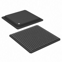
... OUTLINE DIMENSIONS The ADSP-TS101S is available × 19 mm, 484-ball PBGA package with 22 rows of balls (B-484); the DSP also is available × 27 mm, 625-ball PBGA package with 25 rows of balls (B-625). 17.05 16.95 16.85 TOP VIEW 2.50 MAX NOTES: 1. ALL DIMENSIONS ARE IN MILLIMETERS. 2. THE ACTUAL POSITION OF THE BALL GRID IS WITHIN 0. ITS IDEAL POSITION RELATIVE TO THE PACKAGE EDGES ...
Page 44
... ADSP-TS101S 24.20 24.00 23.80 TOP VIEW 2.50 MAX NOTES: 1. ALL DIMENSIONS ARE IN MILLIMETERS. 2. THE ACTUAL POSITION OF THE BALL GRID IS WITHIN 0. ITS IDEAL POSITION RELATIVE TO THE PACKAGE EDGES. 3. CENTER DIMENSIONS ARE NOMINAL. 4. THIS PACKAGE COMPLIES WITH THE JEDEC MS-034 SPECIFICATION, BUT USES TIGHTER TOLERANCES THAN THE MAXIMUMS ALLOWED IN THAT SPECIFICATION ...
Page 45
... ADSP-TS101SAB1-100 –40°C to +85°C ADSP-TS101SAB1Z000 –40°C to +85°C ADSP-TS101SAB1Z100 –40°C to +85°C ADSP-TS101SAB2-000 –40°C to +85°C ADSP-TS101SAB2-100 –40°C to +85°C ADSP-TS101SAB2Z000 –40°C to +85°C ADSP-TS101SAB2Z100 –40°C to +85° indicates 1.2 V and 3.3 V supplies indicates – ...
Page 46
... ADSP-TS101S Rev Page May 2009 ...
Page 47
... Rev Page May 2009 ADSP-TS101S ...
Page 48
... ADSP-TS101S ©2009 Analog Devices, Inc. All rights reserved. Trademarks and registered trademarks are the property of their respective owners. D03164-0-5/09(C) Rev Page May 2009 ...