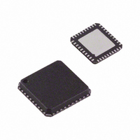
ADV7179KCPZ-REEL Analog Devices Inc, ADV7179KCPZ-REEL Datasheet - Page 17

ADV7179KCPZ-REEL
Manufacturer Part Number
ADV7179KCPZ-REEL
Description
Chip Scale NTSC/PAL Vid Encoder APM I.C.
Manufacturer
Analog Devices Inc
Type
Video Encoderr
Datasheet
1.ADV7179KCPZ.pdf
(52 pages)
Specifications of ADV7179KCPZ-REEL
Applications
Digital Cameras, Mobile Phones, Portable Video
Voltage - Supply, Analog
2.8 V, 3.3 V
Mounting Type
Surface Mount
Package / Case
40-LFCSP
Lead Free Status / RoHS Status
Lead free / RoHS Compliant
Voltage - Supply, Digital
-
Lead Free Status / RoHS Status
Lead free / RoHS Compliant
Other names
ADV7179KCPZ-REELTR
Available stocks
Company
Part Number
Manufacturer
Quantity
Price
Company:
Part Number:
ADV7179KCPZ-REEL
Manufacturer:
TI
Quantity:
69 456
Part Number:
ADV7179KCPZ-REEL
Manufacturer:
ADI/亚德诺
Quantity:
20 000
Vertical Blanking Data Insertion
It is possible to allow encoding of incoming YCbCr data on
those lines of VBI that do not bear line sync or pre-/post-
equalization pulses (see Figure 21 to Figure 32). This mode of
operation is called partial blanking and is selected by setting
MR32 to 1. It allows the insertion of any VBI data (opened VBI)
into the encoded output waveform. This data is present in the
digitized incoming YCbCr data stream, for example. WSS data,
CGMS, VPS, and so on. Alternatively, the entire VBI may be
blanked (no VBI data inserted) on these lines by setting MR32
to 0.
Mode 0 (CCIR-656): Slave Option
(Timing Register 0 TR0 = X X X X X 0 0 0)
The ADV7174/ADV7179 is controlled by the SAV (start active
video) and EAV (end active video) time codes in the pixel data.
All timing information is transmitted using a 4-byte synchro-
RTC
NOTES
1
2
3
F
F
BE WRITTEN TO THE SUBCARRIER FREQUENCY REGISTERS OF THE ADV7174/ADV7179.
SEQUENCE BIT
PAL: 0 = LINE NORMAL, 1 = LINE INVERTED
NTSC: 0 = NO CHANGE
RESET BIT
RESET ADV7174/ADV7179 DDS
SC
SC
PLL INCREMENT BITS 21:0 PLUS BITS 0:9 OF THE SUBCARRIER FREQUENCY REGISTERS. ALL ZEROS SHOULD
PLL INCREMENT IS 22 BITS LONG, VALUE LOADED INTO ADV7174/ADV7179 F
H/LTRANSITION
COUNT START
TIME SLOT: 01
128
COMPOSITE
OR CABLE)
LOW
(e.g., VCR
13
VIDEO
ADV7174/ADV7179
NOT USED IN THE
RESERVED
14 BITS
(e.g., ADV7183A)
DECODER
VIDEO
0
14
Figure 19. RTC Timing and Connections
RESERVED
4 BITS
19
21
Rev. B | Page 17 of 52
CLOCK
SCRESET/RTC
HSYNC
FIELD/VSYNC
P7–P0
AD7174/ADV7179
SC
SAMPLE
nization pattern. A synchronization pattern is sent immediately
before and after each line during active picture and retrace.
Mode 0 is illustrated in Figure 20. The HSYNC , FIELD/ VSYNC ,
and BLANK (if not used) pins should be tied high during this
mode.
Mode 0 (CCIR-656): Master Option
(Timing Register 0 TR0 = X X X X X 0 0 1)
The ADV7174/ADV7179 generates H, V, and F signals required
for the SAV and EAV time codes in the CCIR-656 standard. The
H bit is output on the HSYNC pin, the V bit is output on the
BLANK pin, and the F bit is output on the FIELD/ VSYNC pin.
Mode 0 is illustrated in
The H, V, and F transitions relative to the video waveform are
illustrated in
F
VALID
SC
DDS REGISTER IS
BLUE/COMPOSITE/Pb
PLL INCREMENT
RED/CHROMA/Pr
GREEN/LUMA/Y
SAMPLE
INVALID
Figure 23
1
.
Figure 21
RESERVED
5 BITS
8/LLC
0
(NTSC) and
SEQUENCE
ADV7174/ADV7179
BIT
2
67 68
RESET
BIT
3
Figure 22
RESERVED
(PAL).


