AM29F010B-90EI Spansion Inc., AM29F010B-90EI Datasheet - Page 4
AM29F010B-90EI
Manufacturer Part Number
AM29F010B-90EI
Description
Flash Memory IC
Manufacturer
Spansion Inc.
Datasheets
1.AM29F010B-90PD.pdf
(33 pages)
2.AM29F010B-90PD.pdf
(33 pages)
3.AM29F010B-90EI.pdf
(35 pages)
Specifications of AM29F010B-90EI
Memory Size
1Mbit
Memory Configuration
128K X 8
Ic Interface Type
Parallel
Access Time
90ns
Memory Case Style
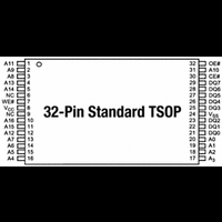
TSOP
No. Of Pins
32
Peak Reflow Compatible (260 C)
No
Supply Voltage
5V
Lead Free Status / RoHS Status
Contains lead / RoHS non-compliant


TABLE OF CONTENTS
Product Selector Guide . . . . . . . . . . . . . . . . . . . . . 4
Block Diagram . . . . . . . . . . . . . . . . . . . . . . . . . . . . . 4
Connection Diagrams . . . . . . . . . . . . . . . . . . . . . . . 5
Pin Configuration . . . . . . . . . . . . . . . . . . . . . . . . . . 7
Logic Symbol . . . . . . . . . . . . . . . . . . . . . . . . . . . . . 7
Ordering Information . . . . . . . . . . . . . . . . . . . . . . . 8
Device Bus Operations . . . . . . . . . . . . . . . . . . . . . . 9
Command Definitions . . . . . . . . . . . . . . . . . . . . . . 12
Write Operation Status . . . . . . . . . . . . . . . . . . . . . 16
November 18, 2002
Requirements for Reading Array Data ..................................... 9
Writing Commands/Command Sequences .............................. 9
Program and Erase Operation Status .................................... 10
Standby Mode ........................................................................ 10
Output Disable Mode .............................................................. 10
Autoselect Mode ..................................................................... 10
Sector Protection/Unprotection ............................................... 11
Hardware Data Protection ...................................................... 11
Reading Array Data ................................................................ 12
Reset Command ..................................................................... 12
Autoselect Command Sequence ............................................ 12
Byte Program Command Sequence ....................................... 12
Chip Erase Command Sequence ........................................... 13
Sector Erase Command Sequence ........................................ 13
Erase Suspend/Erase Resume Commands ........................... 14
Command Definitions ............................................................. 15
DQ7: Data# Polling ................................................................. 16
DQ6: Toggle Bit I .................................................................... 16
Reading Toggle Bit DQ6 ......................................................... 17
Table 1. Am29F010B Device Bus Operations .................................9
Table 2. Am29F010B Sector Addresses Table ...............................10
Table 3. Am29F010B Autoselect Codes (High Voltage Method) ....11
Low V
Write Pulse “Glitch” Protection ........................................................11
Logical Inhibit ..................................................................................11
Power-Up Write Inhibit ....................................................................11
Figure 1. Program Operation ..........................................................13
Figure 2. Erase Operation ...............................................................14
Table 4. Am29F010B Command Definitions ...................................15
Figure 3. Data# Polling Algorithm ...................................................16
Figure 4. Toggle Bit Algorithm .........................................................17
CC
Write Inhibit ......................................................................11
Am29F010B
Absolute Maximum Ratings . . . . . . . . . . . . . . . . 19
Operating Ranges . . . . . . . . . . . . . . . . . . . . . . . . 19
DC Characteristics . . . . . . . . . . . . . . . . . . . . . . . . 20
Test Conditions . . . . . . . . . . . . . . . . . . . . . . . . . . 22
Key to Switching Waveforms . . . . . . . . . . . . . . . 22
AC Characteristics . . . . . . . . . . . . . . . . . . . . . . . . 23
Erase and Programming Performance . . . . . . . 28
Latchup Characteristic . . . . . . . . . . . . . . . . . . . . 29
TSOP Pin Capacitance . . . . . . . . . . . . . . . . . . . . 29
PLCC and PDIP Pin Capacitance . . . . . . . . . . . . 29
Data Retention . . . . . . . . . . . . . . . . . . . . . . . . . . . 29
Physical Dimensions . . . . . . . . . . . . . . . . . . . . . . 30
Revision Summary . . . . . . . . . . . . . . . . . . . . . . . . 34
DQ5: Exceeded Timing Limits ................................................ 17
DQ3: Sector Erase Timer ....................................................... 18
Erase and Program Operations ......................................................... 24
Erase and Program Operations ......................................................... 27
PD 032—32-Pin Plastic DIP ................................................... 30
PL 032—32-Pin Plastic Leaded Chip Carrier ......................... 31
TS 032—32-Pin Standard Thin Small Outline Package ......... 32
TSR 032—32-Pin Standard Thin Small Outline Package ....... 33
Revision A (August 12, 1999) ................................................. 34
Revision A+1 (September 22, 1999) ...................................... 34
Revision A+2 (September 27, 1999) ...................................... 34
Revision B (November 12, 1999) ............................................ 34
Revision C (November 28, 2000) ........................................... 34
Table 5. Write Operation Status ..................................................... 18
Figure 5. Maximum Negative Overshoot Waveform ...................... 19
Figure 6. Maximum Positive Overshoot Waveform ........................ 19
Figure 7. Test Setup ....................................................................... 22
Table 6. Test Specifications ........................................................... 22
Figure 8. Read Operations Timings ............................................... 23
Figure 9. Program Operation Timings ............................................ 25
Figure 10. Chip/Sector Erase Operation Timings .......................... 25
Figure 11. Data# Polling Timings (During Embedded Algorithms) . 26
Figure 12. Toggle Bit Timings (During Embedded Algorithms) ...... 26
Alternate CE# Controlled Writes .................................................... 27
Figure 13. Alternate CE# Controlled Write Operation Timings ...... 28
3
Related parts for AM29F010B-90EI
Image
Part Number
Description
Manufacturer
Datasheet
Request
R

Part Number:
Description:
Manufacturer:
Meet Spansion Inc.
Datasheet:
Part Number:
Description:
Manufacturer:
Meet Spansion Inc.
Datasheet:

Part Number:
Description:
IC, FLASH, 1MBIT, 70NS, LCC-32
Manufacturer:
Spansion Inc.
Datasheet:

Part Number:
Description:
IC, FLASH, 1MBIT, 45NS, TSOP-32
Manufacturer:
Spansion Inc.
Datasheet:

Part Number:
Description:
IC, FLASH, 1MBIT, 55NS, TSOP-32
Manufacturer:
Spansion Inc.
Datasheet:
Part Number:
Description:
IC, FLASH, 1MBIT, 55NS, LCC-32
Manufacturer:
Spansion Inc.
Datasheet:

Part Number:
Description:
IC, FLASH, 1MBIT, 70NS, TSOP-32
Manufacturer:
Spansion Inc.
Datasheet:
Part Number:
Description:
IC, FLASH, 1MBIT, 70NS, LCC-32
Manufacturer:
Spansion Inc.
Datasheet:
Part Number:
Description:
FLASH NON-VOLATILE MEMORY
Manufacturer:
Spansion Inc.
Datasheet:

Part Number:
Description:
Flash Memory IC
Manufacturer:
Spansion Inc.
Datasheet:
Part Number:
Description:
Flash Memory IC
Manufacturer:
Spansion Inc.
Datasheet:
Part Number:
Description:
Flash Memory IC
Manufacturer:
Spansion Inc.
Datasheet:
Part Number:
Description:
Flash Memory IC
Manufacturer:
Spansion Inc.
Datasheet:
Part Number:
Description:
Flash Memory IC
Manufacturer:
Spansion Inc.
Datasheet: