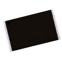
AM29LV641DH120REI Spansion Inc., AM29LV641DH120REI Datasheet - Page 12

AM29LV641DH120REI
Manufacturer Part Number
AM29LV641DH120REI
Description
Flash Memory IC
Manufacturer
Spansion Inc.
Specifications of AM29LV641DH120REI
Memory Configuration
4M X 16
Ic Interface Type
Parallel
Access Time
120ns
Memory Case Style
TSOP
No. Of Pins
48
Mounting Type
Surface Mount
Peak Reflow Compatible (260 C)
No
Supply Voltage
3V
Lead Free Status / RoHS Status
Contains lead / RoHS non-compliant
DEVICE BUS OPERATIONS
This section describes the requirements and use of
the device bus operations, which are initiated through
the internal command register. The command register
itself does not occupy any addressable memory loca-
tion. The register is a latch used to store the com-
mands, along with the address and data information
needed to execute the command. The contents of the
Legend: L = Logic Low = V
A
Notes:
1. Addresses are A21:A0. Sector addresses are A21:A15.
2. The sector protect and sector unprotect functions may also be implemented via programming equipment. See the “Sector Group
3. If WP# = V
4. D
VersatileIO
The VersatileIO™ (V
to set the voltage levels that the device generates and
tolerates on CE# and DQ I/Os to the same voltage
level that is asserted on V
configurations (1.8–2.9 V and 3.0–5.0 V) for operation
in various system environments.
For example, a V
the 5 volt level, driving and receiving signals to and
from other 5 V devices on the same data bus.
September 20, 2002
Read
Write (Program/Erase)
Accelerated Program
Standby
Output Disable
Reset
Sector Group Protect (Note 2)
Sector Group Unprotect
(Note 2)
Temporary Sector Group
Unprotect
IN
= Address In, D
Protection and Unprotection” section.
determined by the method described in “Sector Group Protection and Unprotection”. All sectors are unprotected when shipped
from the factory (The SecSi Sector may be factory protected depending on version ordered.)
IN
or D
Operation
OUT
IL
, the first or last sector remains protected. If WP# = V
as required by command sequence, data polling, or sector protect algorithm (see Figure 2).
(V
IN
I/O
= Data In, D
IO
IO
of 4.5–5.0 volts allows for I/O at
) Control
) control allows the host system
IL
, H = Logic High = V
IO
V
0.3 V
CE#
. V
CC
OUT
X
X
L
L
L
L
L
L
IO
= Data Out
is available in two
OE#
H
H
X
H
X
H
H
X
L
Table 1. Device Bus Operations
WE# RESET#
Am29LV640D/Am29LV641D
H
H
X
X
X
L
L
L
L
IH
, V
ID
V
= 8.5–12.5 V, V
0.3 V
V
V
V
CC
H
H
H
H
L
ID
ID
ID
(Note 3)
(Note 3)
IH
WP#
register serve as inputs to the internal state machine.
The state machine outputs dictate the function of the
device. Table 1 lists the device bus operations, the in-
puts and control levels they require, and the resulting
output. The following subsections describe each of
these operations in further detail.
Requirements for Reading Array Data
To read array data from the outputs, the system must
drive the CE# and OE# pins to V
control and selects the device. OE# is the output con-
trol and gates array data to the output pins. WE#
should remain at V
The internal state machine is set for reading array data
upon device power-up, or after a hardware reset. This
ensures that no spurious alteration of the memory
content occurs during the power transition. No com-
mand is necessary in this mode to obtain array data.
Standard microprocessor read cycles that assert valid
addresses on the device address inputs produce valid
, the first or last sector will be protected or unprotected as
X
X
X
X
H
H
H
HH
= 11.5–12.5 V, X = Don’t Care, SA = Sector Address,
ACC
V
H
X
X
X
X
X
X
X
HH
IH
.
A1 = H, A0 = L
A1 = H, A0 = L
SA, A6 = H,
Addresses
SA, A6 = L,
(Note 2)
A
A
A
A
X
X
X
IN
IN
IN
IN
IL
. CE# is the power
(Note 4)
(Note 4)
(Note 4)
(Note 4)
(Note 4)
High-Z
High-Z
High-Z
DQ0–
DQ15
D
OUT
11


