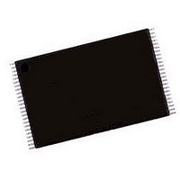
AM29LV641DL120REI Spansion Inc., AM29LV641DL120REI Datasheet - Page 28

AM29LV641DL120REI
Manufacturer Part Number
AM29LV641DL120REI
Description
Flash Memory IC
Manufacturer
Spansion Inc.
Specifications of AM29LV641DL120REI
Memory Size
64Mbit
Memory Configuration
4M X 16
Ic Interface Type
Parallel
Access Time
120ns
Memory Case Style
TSOP
No. Of Pins
48
Operating Temperature Range
-40°C To +85°C
Termination Type
SMD
Available stocks
Company
Part Number
Manufacturer
Quantity
Price
When the Embedded Erase algorithm is complete, the
device returns to the read mode and addresses are no
longer latched. The system can determine the status
of the erase operation by using DQ7, DQ6, DQ2, or
RY/BY#. Refer to the Write Operation Status section
for information on these status bits.
Any commands written during the chip erase operation
are ignored. However, note that a hardware reset im-
mediately terminates the erase operation. If that oc-
curs, the chip erase command sequence should be
reinitiated once the device has returned to reading
array data, to ensure data integrity.
Figure 4 illustrates the algorithm for the erase opera-
tion. Refer to the Erase and Program Operations ta-
bles in the AC Characteristics section for parameters,
and Figure 17 section for timing diagrams.
Sector Erase Command Sequence
Sector erase is a six bus cycle operation. The sector
erase command sequence is initiated by writing two
unlock cycles, followed by a set-up command. Two ad-
ditional unlock cycles are written, and are then fol-
lowed by the address of the sector to be erased, and
the sector erase command. Table 10 shows the ad-
dress and data requirements for the sector erase com-
mand sequence.
The device does not require the system to preprogram
prior to erase. The Embedded Erase algorithm auto-
matically programs and verifies the entire memory for
an all zero data pattern prior to electrical erase. The
system is not required to provide any controls or tim-
ings during these operations.
After the command sequence is written, a sector erase
time-out of 50 µs occurs. During the time-out period,
additional sector addresses and sector erase com-
mands may be written. Loading the sector erase buffer
may be done in any sequence, and the number of sec-
tors may be from one sector to all sectors. The time
between these additional cycles must be less than 50
µs, otherwise erasure may begin. Any sector erase
address and command following the exceeded
time-out may or may not be accepted. It is recom-
mended that processor interrupts be disabled during
this time to ensure all commands are accepted. The
interrupts can be re-enabled after the last Sector
Erase command is written. Any command other than
S e ct o r E ra se o r E ra s e S u sp en d d u r in g th e
time-out period resets the device to the read
mode. The system must rewrite the command se-
quence and any additional addresses and commands.
The system can monitor DQ3 to determine if the sec-
tor erase timer has timed out (See the section on DQ3:
Sector Erase Timer.). The time-out begins from the ris-
ing edge of the final WE# pulse in the command
sequence.
September 20, 2002
Am29LV640D/Am29LV641D
When the Embedded Erase algorithm is complete, the
device returns to reading array data and addresses
are no longer latched. The system can determine the
status of the erase operation by reading DQ7, DQ6,
DQ2, or RY/BY#. Note that while the Embedded Erase
operation is in progress, the system can read data
from the non-erasing sector. Refer to the Write Opera-
tion Status section for information on these status bits.
Once the sector erase operation has begun, only the
Erase Suspend command is valid. All other com-
mands are ignored. However, note that a hardware
reset immediately terminates the erase operation. If
that occurs, the sector erase command sequence
should be reinitiated once the device has returned to
reading array data, to ensure data integrity.
Figure 4 illustrates the algorithm for the erase opera-
tion. Refer to the Erase and Program Operations ta-
bles in the AC Characteristics section for parameters,
and Figure 17 section for timing diagrams.
Erase Suspend/Erase Resume
Commands
The Erase Suspend command, B0h, allows the sys-
tem to interrupt a sector erase operation and then read
data from, or program data to, any sector not selected
for erasure. This command is valid only during the
sector erase operation, including the 50 µs time-out
period during the sector erase command sequence.
The Erase Suspend command is ignored if written dur-
ing the chip erase operation or Embedded Program
algorithm.
When the Erase Suspend command is written during
the sector erase operation, the device requires a max-
imum of 20 µs to suspend the erase operation. How-
ever, when the Erase Suspend command is written
during the sector erase time-out, the device immedi-
ately terminates the time-out period and suspends the
erase operation.
After the erase operation has been suspended, the
device enters the erase-suspend-read mode. The sys-
tem can read data from or program data to any sector
not selected for erasure. (The device “erase sus-
pends” all sectors selected for erasure.) Reading at
any address within erase-suspended sectors pro-
duces status information on DQ7–DQ0. The system
can use DQ7, or DQ6 and DQ2 together, to determine
if a sector is actively erasing or is erase-suspended.
Refer to the Write Operation Status section for infor-
mation on these status bits.
After an erase-suspended program operation is com-
plete, the device returns to the erase-suspend-read
mode. The system can determine the status of the
program operation using the DQ7 or DQ6 status bits,
just as in the standard word program operation.
27


